AI technical title is built by Patsnap AI team. It summarizes the technical point description of the patent document.
A manufacturing method, semiconductor technology, applied in semiconductor/solid-state device manufacturing, semiconductor devices, semiconductor/solid-state device components, etc., can solve problems such as poor production capacity and time required for formation
Inactive Publication Date: 2005-02-09
SOCIONEXT INC
View PDF0 Cites 7 Cited by
Summary
Abstract
Description
Claims
Application Information
AI Technical Summary
This helps you quickly interpret patents by identifying the three key elements:
Problems solved by technology
Method used
Benefits of technology
Problems solved by technology
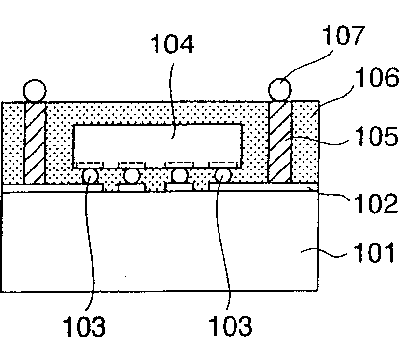
[0007] but, figure 1 The terminal 105 shown is formed on the wiring 102 by electroplating, so the formation of the terminal 105 takes time, and the productivity of CSP formation is poor.
Method used
Image
Click on the blue label to locate the original text in one second.
Reading with bidirectional positioning of images and text.
Examples
Embodiment approach 1
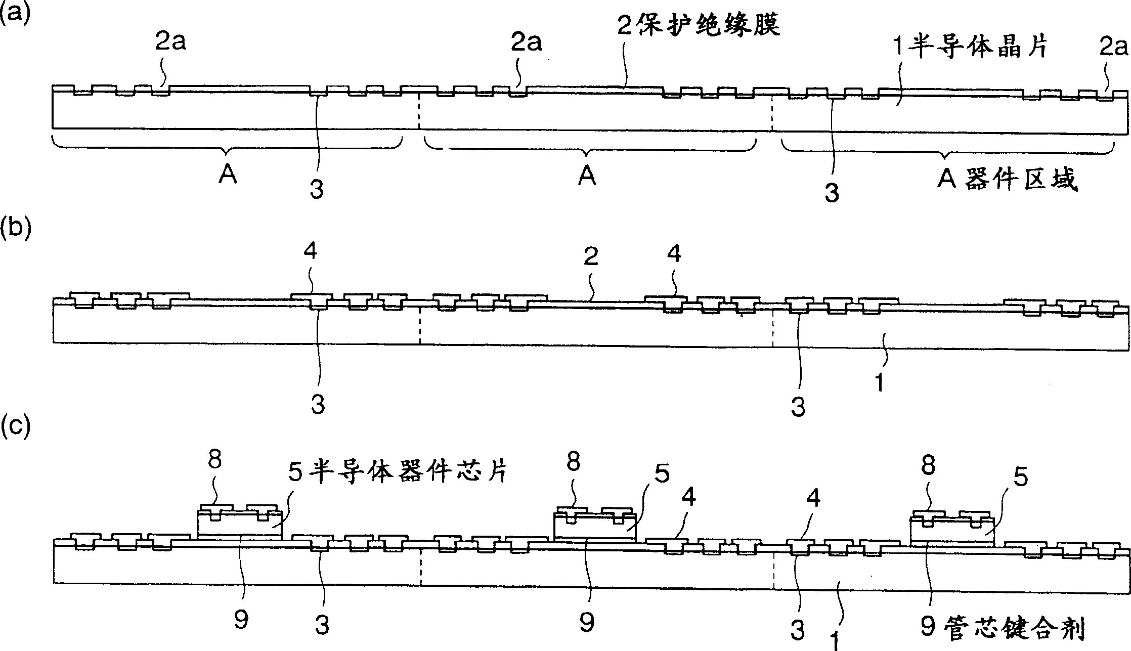
[0037] Figure 2 to Figure 5 It is a sectional view showing the formation process of the multi-chip package (MCP) in Embodiment 1 of this invention.
[0038] First, if figure 2 As shown in (a), a semiconductor wafer 1 in which first semiconductor circuits (not shown) are formed on a plurality of device regions A is prepared. Semiconductorwafer 1 such as Image 6 As shown in the partial enlarged view of (a), there is a protective insulating film 2 on the upper surface, and an opening 2a exposing the first terminal (conductive pad) 3 is formed on the protective insulating film 2, and the first terminal and the semiconductor Internal wiring (not shown) of the device is electrically connected. The first terminal 3 is formed of aluminum, copper, or the like.
[0039] Furthermore, the semiconductor wafer 1 is, for example, a silicon wafer, and is cut into individual first semiconductor circuits in a post-process, and is divided into units of device regions A. As shown in FIG. ...
Embodiment approach 2
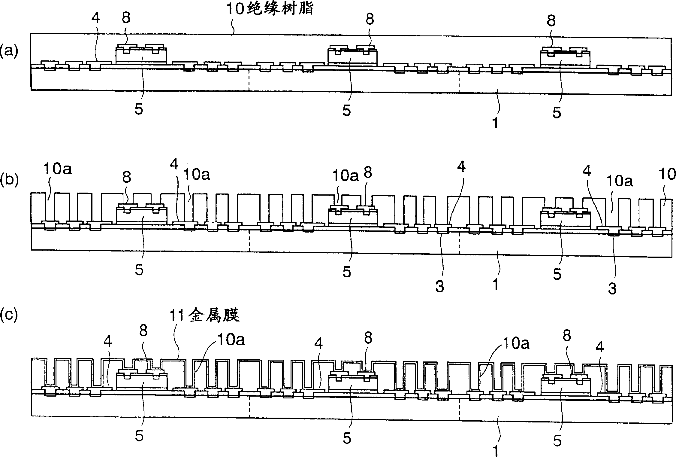
[0067] In Embodiment 1, after the via 11 a and the rewiring pattern 11 b are formed, the buried insulating layer 12 is formed in the via hole 10 a, and then the resin cover film 13 is formed on the resin insulating layer 10 . However, it is also possible to form the buried insulating layer 12 and the resin cover film 13 at the same time.
[0068] For example Figure 9 As shown in (a), after the photosensitive resin film 15, such as epoxy resin, is coated simultaneously in the via hole 10a and on the resin insulating layer 10, the exposure and development of the resin film 15 form the third rewiring pattern 11b. The opening 15a through which the terminal portion is exposed.
[0069] later as Figure 9 As shown in (b), the external terminal 14 is joined to the rewiring pattern 11b through the opening 15a of the resin film 15 .
[0070] According to this embodiment, the epoxy resin in the via hole 10a is used as the buried insulating layer, and the epoxy resin on the resin ins...
Embodiment approach 3
[0073] When the first rewiring pattern 3 is not formed on the semiconductor wafer 1 described in Embodiment 1, the following steps are employed.
[0074] First, if Figure 11 As shown in (a) and (b), on the terminal 3 in the opening 2a of the protective insulating film 2 on the semiconductor wafer 1, the electroless plating method is used to selectively form 3-5 μm thickness made of nickelphosphorus (NiP), nickel , gold, etc. to form a coating conductive layer 16.
[0075] later as Figure 11 As shown in (c), the first semiconductor device chip 5 is mounted on the semiconductor wafer 1 by the same method as in the first embodiment. As the first semiconductor device chip 5, a device having a structure in which a NiP-coated conductive film 17 is formed on the second terminal 7 of the protective insulating film 6 without forming a rewiring pattern is used.
[0076] Then as Figure 12 As shown in (a), a resin insulating layer 10 is formed on the semiconductor wafer 1 so as to...
PUM
Abstract
A semiconductor device comprising a first semiconductorchip having first terminals on one side thereof, a second semiconductorchip larger than the first semiconductor chip being stacked thereon and having second terminals on one side thereof, an insulation film formed on the second semiconductor chip to cover the first semiconductor chip, a plurality of holes made in the insulation film at least in the peripheral region of the first semiconductor chip, vias made in film shape on the inner circumferential face and the bottom face of the holes and connected electrically with the second terminals of the second semiconductor chip, a wiring pattern formed on the upper surface of the insulation film, and external terminals connected onto the wiring pattern. A semiconductor device copmrising a first semiconductor chip having first terminals on one side thereof, a second semiconductor chip larger than the first semiconductor chip being stacked thereon and having second terminals on one side thereof, an insulation film formed on the second semiconductor chip to cover the first semiconductor chip, a plurality of holes made in the insulation film at least in the peripheral region of the first semiconductor chip.
Description
technical field [0001] The present invention relates to a semiconductor device and its manufacturing method, and more particularly to a semiconductor device having a plurality of semiconductor chips and its manufacturing method. Background technique [0002] For the next generation of portable information terminal equipment including mobile phones and mobile PCs, the improvement of miniaturization, light weight and thinness has become a primary issue. Therefore, in order to enhance the competitiveness of portable information terminals, which are expected to grow rapidly in the future, it is important to develop high-density mounting technologies that can achieve further reduction in size, weight, and thickness. [0003] As high-density mounting technologies, there are various technologies such as flip-chip mounting, multi-chip modules, and laminated substrates. Furthermore, from the need to carry multiple functions in a package, technology development of a chip-scale packag...
Claims
Application Information
Patent Timeline
Application Date:The date an application was filed.
Publication Date:The date a patent or application was officially published.
First Publication Date:The earliest publication date of a patent with the same application number.
Issue Date:Publication date of the patent grant document.
PCT Entry Date:The Entry date of PCT National Phase.
Estimated Expiry Date:The statutory expiry date of a patent right according to the Patent Law, and it is the longest term of protection that the patent right can achieve without the termination of the patent right due to other reasons(Term extension factor has been taken into account ).
Invalid Date:Actual expiry date is based on effective date or publication date of legal transaction data of invalid patent.

