Method for mfg. printed circuitboard

A technology for printed circuit boards and manufacturing methods, applied in printed circuit manufacturing, printed circuits, removal of conductive materials by chemical/electrolytic methods, etc., capable of solving excessive etching undercuts, increased number of processes, and reduced circuit width, etc. question

Inactive Publication Date: 2005-03-09
MITSUBISHI GAS CHEM CO INC
View PDF6 Cites 8 Cited by
  • Summary
  • Abstract
  • Description
  • Claims
  • Application Information

AI Technical Summary

Problems solved by technology

[0005] However, since steps such as forming a thin metal film other than copper and peeling are required, there is a problem that the number of steps increases
[0006] Also, if the circuit width is narrowed, the time to remove the electroless copper plating as the seed layer differs greatly between the place where the distance between the wirings is wide and the place where the distance between the wirings is narrow. The problem that the width of the circuit becomes smaller than the width of the circuit where the distance is narrow
[0007] Further, since etching is performed with an etching amount greater than the thickness of the electroless copper plating of the seed layer, undercut (under cut) caused by excessive etching is prone to occur.
So far, there have been reports of using alkali and amine etching solutions without undercutting, but the problem is that the undercut looks small on the outside due to the large reduction in circuit width.

Method used


Image

  • Method for mfg. printed circuitboard

Examples


Embodiment 1

[0054] 10 L of an etching solution consisting of 1% by weight of hydrogen peroxide, 4% by weight of sulfuric acid, 0.01% by weight of 1H-tetrazole, copper at a concentration of 20 g / L (liter), and water was prepared as the remainder.

[0055] [Measurement of etching rate]

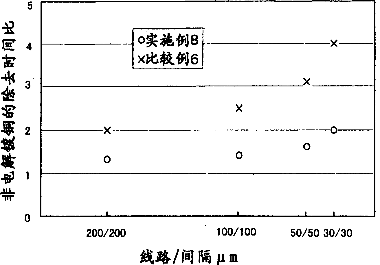
[0056] A base plate (150×150 mm) on which 2 μm thick electroless copper plating was formed and a base plate (150×150 mm) on which 20 μm thick electrolytic copper plating was formed were produced. Using a spray etching machine, at a spray pressure of 0.1 MPa and a treatment temperature of 30° C., the electroless copper-plated base plate was etched for 15 seconds, and the electrolytic copper-plated base plate was etched for 30 seconds. The amount of etching was calculated from the weight difference of the substrate before and after the treatment. The dissolution rate ratio (etching rate ratio) is represented by the ratio of the etching amount per unit time obtained by dividing the etching amount of each proc...

Embodiment 2

[0060] In addition to using an etching solution consisting of 1.5% by weight of hydrogen peroxide, 5% by weight of sulfuric acid, 0.01% by weight of 1,2,4-triazole, copper with a concentration of 20g / L, and the remainder consisting of water, the same as the implementation The same experiment was carried out in Example 1.

Embodiment 3

[0062] Except using hydrogen peroxide by 1% by weight, sulfuric acid of 3% by weight, triethylenetetramine of 2% by weight, the copper of concentration 20g / L, the remainder is made up of water, same as Example 1 conduct experiment.


PUM


Abstract

To provide a method for reducing a wiring width in the formation of a copper wiring by the semi-additive method of a printed circuit board, etc., suppressing an undercut and further forming a uniform wiring width in a plane. The method for manufacturing the printed circuit board having the fine wiring of a line/space of 50 [mu]m/50 [mu]m or less using the semi-additive method includes a step of processing with an etchant liquid in which an etching speed of non-electrolytic copper plating of a seed layer is twice as fast as the etching speed of the electrolytic copper plating, and non-electrolytic copper plating removing time in space of the fine wiring having the line/space of 50 [mu]m/50 [mu]m or less is larger than 50 [mu]m or less is three times as fast as the non-electrolytic copper plating removing time in the space larger than 50 [mu]m, and manufacturing of the printed circuit board.

Description

technical field [0001] The present invention relates to a method of manufacturing printed circuit boards. In particular, it relates to a method of manufacturing a printed wiring board including a step of etching copper by a semi-additive method. Background technique [0002] In the manufacturing process of printed circuit boards, there is a semi-additive method as a method of forming wiring. In the formation method of this circuit, a seed layer of electroless copper plating of about 0.5-2 μm is formed on the electrical insulating layer, and an electroplating protective layer is coated on the seed layer, and then through exposure and development processes, and finally only Remove the electroplating protection layer where the conductor pattern is formed. Electrolytic copper plating is performed here to form a conductor circuit layer, the protective layer is peeled off, and the unused electroless copper plating is removed by etching to form wiring. As etchant, what used in t...

Claims


Application Information

Patent Timeline
Patent Type & Authority Applications(China)
IPC IPC(8): C23F1/18C09K13/04C23F1/00H05K3/06
CPCC23F1/18H05K3/067H05K3/108
Inventor 细见彰良高桥健一
Owner MITSUBISHI GAS CHEM CO INC
Why Eureka
Try Eureka