Method for producing semiconductor device and cleaning device for resist stripping

A manufacturing method and semiconductor technology, applied in semiconductor/solid-state device manufacturing, semiconductor device, patterned surface photoplate making process, etc., can solve the problems of particle or metal impurity adhesion, etc., achieve adhesion suppression, sufficient yield, The effect of excellent device characteristics

Inactive Publication Date: 2005-06-01
RENESAS ELECTRONICS CORP
View PDF1 Cites 12 Cited by
  • Summary
  • Abstract
  • Description
  • Claims
  • Application Information

AI Technical Summary

Problems solved by technology

[0011] In recent years, due to the pattern micro-manufacturing brought about by the high integration of semiconductor devices, higher cleanliness is required, and conventional immersion-type cleaning methods cannot handle this situation, thus the problem of particles or metal impurities adhering to the wafer surface become significant

Method used


Image

  • Method for producing semiconductor device and cleaning device for resist stripping
  • Method for producing semiconductor device and cleaning device for resist stripping
  • Method for producing semiconductor device and cleaning device for resist stripping

Examples


no. 1 example

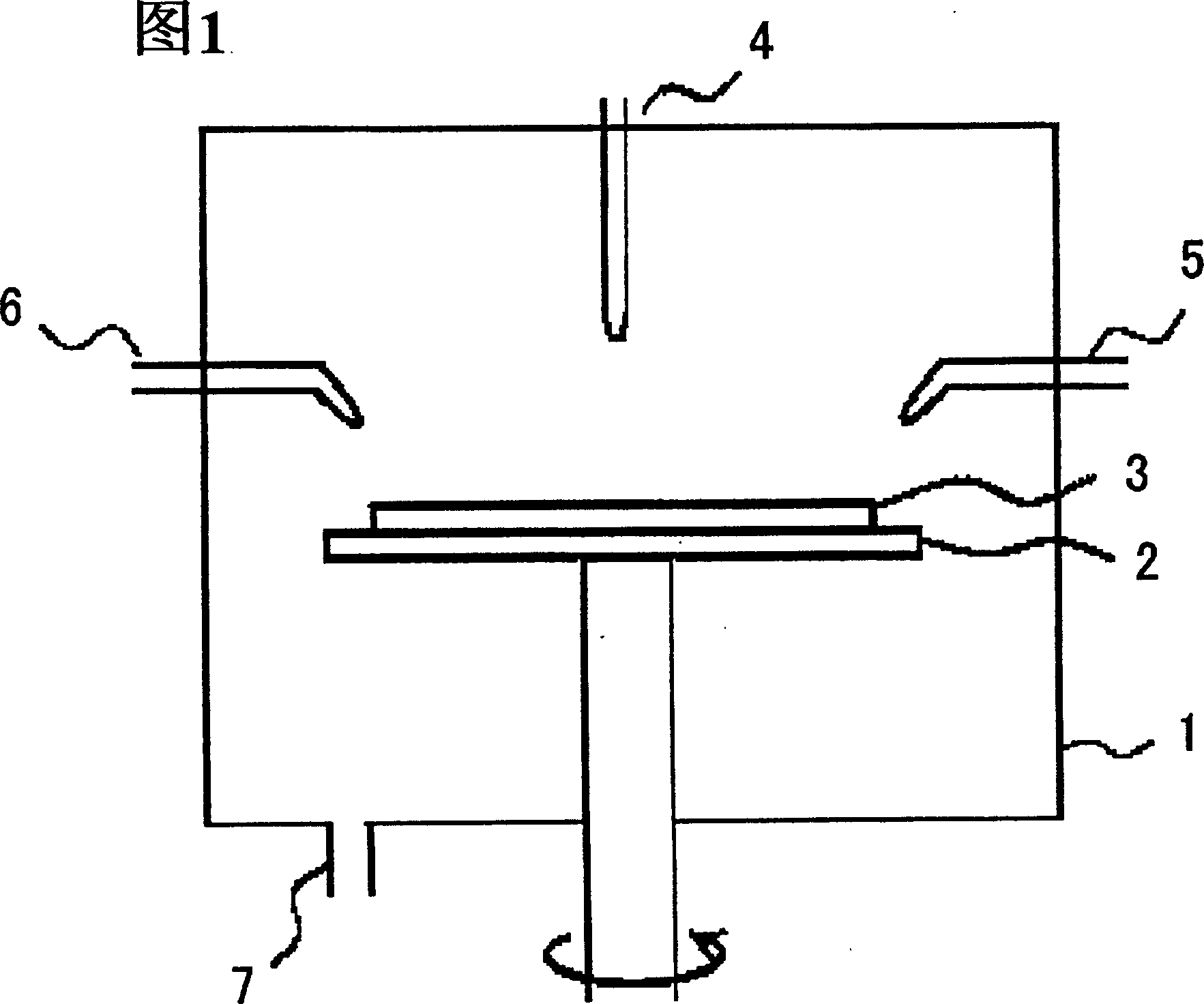
[0099]FIG. 11 shows a schematic structural diagram of a substrate processing apparatus 100 according to an embodiment. The substrate processing apparatus 100 is provided with a processing chamber 102, including a substrate mount table 104, a first container 126 containing a first liquid provided to the surface of a semiconductor substrate 106, a container containing a second liquid provided to the surface of a semiconductor substrate 106, A second container 130 of liquid, a mixing portion 114, communicates with the first container 126 and the second container 130 to produce the mixture while mixing the first and second liquids provided by these containers, and a nozzle 112, in communication with the mixing portion 114, provides the mixture to the surface of the semiconductor substrate 106 , and a conduit 115 connects a mixing section 114 to a nozzle 112 to introduce the mixture from the mixing section 114 into the nozzle 112 . At the periphery of the pipeline 115, a pipeline h...

no. 2 example

[0138] This embodiment illustrates providing the semiconductor substrate 106 with a mixture sprayed by two nozzles. FIG. 14 shows an example of a substrate processing apparatus 100 according to an embodiment. 15A, 15B are views showing the positional relationship between the nozzles 112a, 112b and the semiconductor substrate 106 shown in FIG. 14 . Except for the nozzle structure, the device structure of this embodiment is the same as the device structure shown in the first embodiment. The point of setting the heater around the pipe 115 and the nozzle 112 is the same as indicated in the first embodiment.

[0139] As shown in FIGS. 15A and 15B , the nozzle 112 a sprays the mixture to the end portion of the semiconductor substrate 106 , and the nozzle 112 b sprays the mixture to the center portion of the semiconductor substrate 106 . The nozzle is prepared at an angle "a" to the substrate surface and an angle "b" to the tangential direction of the substrate.

[0140] In this e...

no. 3 example

[0143] In this embodiment, an example in which the mixture is sprayed onto the semiconductor substrate 106 is shown. FIG. 16 shows an example of the substrate processing apparatus 100 in the embodiment. Except for the nozzle structure, the device structure of this embodiment is the same as the device structure shown in the first embodiment. Figure 17 The pipe 115 and heater points around the nozzle 112 shown in are the same as in the first embodiment. As shown in the figure, in this device, the nozzle 112 can move due to the control of the moving part 140 . The nozzle 112 is constructed to spray the mixture while moving the sprayed portion from the center of the substrate to the peripheral portion. In the above structure, within the processed surface of the semiconductor substrate 106, the temperature becomes uniform, whereby the resist stripping efficiency becomes uniform. Although the present embodiment shows that the processing liquid is made high temperature by heat ge...


PUM

PropertyMeasurementUnit
widthaaaaaaaaaa
lengthaaaaaaaaaa

Abstract

A semiconductor device manufacturing method and a cleaning apparatus for stripping a resist provide a semiconductor device having excellent element characteristics with a sufficient yield in the following manner, after dry etching of a photolithography process, the resist is removed by wet cleaning agent, and sufficiently removes particles or metal impurities without damaging fine patterns. A method for manufacturing a semiconductor device includes forming a resist pattern on a film provided for a semiconductor substrate, forming a fine pattern of a conductive film using the resist pattern as a mask while performing dry etching, supplying a resist stripping solution to The fine pattern formation surface of the semiconductor substrate is processed by a single wafer system to remove the resist pattern, and to perform the rinsing process of the semiconductor substrate.

Description

[0001] This application is based on Japanese Patent Applications No. 2003-394249 and No. 2004-324601, the contents of which are incorporated herein by reference. technical field [0002] The present invention relates to a manufacturing method of a semiconductor device and a cleaning device for removing a resist using the same method. Background technique [0003] Usually in the manufacture of a semiconductor device, fine pattern formation of a gate electrode or the like is performed in such a manner that a resist film is formed on a conductive film provided on a semiconductor substrate, and then the resist obtained by patterning the resist The resist pattern of the etchant film is used as a mask for dry etching, and the conductive film is patterned into a predetermined size and shape. As a technique for stripping the resist after patterning, so-called SPM cleaning using a mixed solution of sulfuric acid and hydrogen peroxide, followed by rinsing treatment with pure water is ...

Claims


Application Information

Patent Timeline
Patent Type & Authority Applications(China)
IPC IPC(8): H01L29/423G03F7/00G03F7/16G03F7/42H01L21/00H01L21/027H01L21/304H01L21/311H01L29/49
CPCG03F7/162G03F7/422G03F7/423H01L21/31133
Inventor 清水裕司铃木达也河野通久
Owner RENESAS ELECTRONICS CORP
Why Eureka
Try Eureka