Plasma processing technique for reducing MOCVD TiN film thickness on through-hole side wall

A plasma and processing technology, applied in the field of integrated circuit chip manufacturing, can solve the problems of increased interconnect resistance, high film, CD loss, etc., and achieve the effect of reducing device damage

Inactive Publication Date: 2005-06-29
SHANGHAI HUA HONG GROUP +1
View PDF0 Cites 2 Cited by
  • Summary
  • Abstract
  • Description
  • Claims
  • Application Information

AI Technical Summary

Problems solved by technology

A process problem with existing MOCVD techniques is that during the plasma gas treatment step, the TN barrier layer on the inner sidewall of the hole is barely treated, and its thickness accounts for ~10% of the hole diameter, causing CD loss, interconnect resistance raised
Compared with PVD TiN film, the disadvantage of MOCVD TiN is that the film contains higher impurities such as C and O, which cause the via resistance to be 10~15% higher than that of PVD TiN.

Method used


Image

  • Plasma processing technique for reducing MOCVD TiN film thickness on through-hole side wall
  • Plasma processing technique for reducing MOCVD TiN film thickness on through-hole side wall

Examples


Embodiment Construction

[0030] The implementation steps of this technology are as follows:

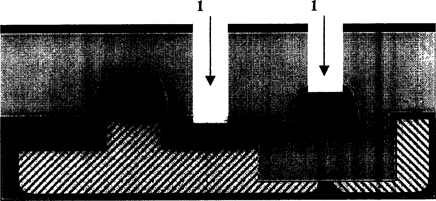
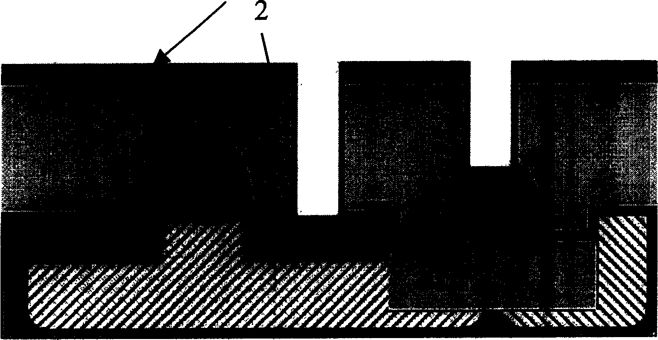
[0031] 1. Etching and cleaning of metal interconnection holes on silicon wafers;

[0032] 2. Deposition of MOCVD TiN film;

[0033] 3. After completion, continue with plasma post-processing. The process steps are: the CVD chamber is fed with N 2 、H 2 and Ar, boosted to 5, 10 or 15 Tor; H 2 :N 2 : Ar=1:1:0.01 or H 2 :N 2 : Ar=1:3:0.001; the gas plasmaization power is controlled at 400, 500 or 750W; the processing time can be between 10 and 20S;

[0034] 4. After step 1 is completed, exhaust the reaction chamber to 10mT;

[0035] 5. Continue to step 3;

[0036] 6. After completing step 5, exhaust the system to 10-7mT;

[0037] 7. The equipment is restored to the state of waiting for manufacture.


PUM


Abstract

This invention belongs to integration circuit process technique field, which in detail is a plasm process to decrease the MOCVD TiN film thickness of the hole sidewall. The current process, the Tin film on the inner sidewall of holes cannot be processed with its thickness of ten percent only to make the resistance increase when in plasm gas process.

Description

technical field [0001] The invention belongs to the technical field of integrated circuit chip manufacturing, and specifically relates to a post-treatment process for reducing the thickness of a TiN film on the side wall of a through hole and removing impurities such as C and O in the TiN film, so as to reduce the resistance of the through hole and reduce the RC delay. Background technique [0002] With the rapid development of integrated circuit manufacturing technology, the main factor restricting the speed of the circuit has changed from the gate delay (gated delay) to the RC delay caused by the resistance (R) of the connection and the capacitance (C) between the connections, thus reducing RC delay is an urgent and important work. [0003] In the current aluminum metal interconnection technology, the aluminum lines are formed by etching, and the aluminum lines of adjacent layers are connected by tungsten in the through holes. And a continuous and complete TiN barrier la...

Claims


Application Information

Patent Timeline
Patent Type & Authority Applications(China)
IPC IPC(8): H01L21/28H01L21/3105H01L21/321H01L21/768
Inventor 朱建军
Owner SHANGHAI HUA HONG GROUP
Why Eureka
Try Eureka