

Method for making organic LED
A technology of light-emitting diodes and manufacturing methods, which is applied in semiconductor/solid-state device manufacturing, electrical components, electric solid-state devices, etc., and can solve problems such as low device efficiency, difficulty in adjusting the light-emitting color of devices, and limiting the application range of organic light-emitting diodes.
- Summary
- Abstract
- Description
- Claims
- Application Information
AI Technical Summary
Problems solved by technology
Method used
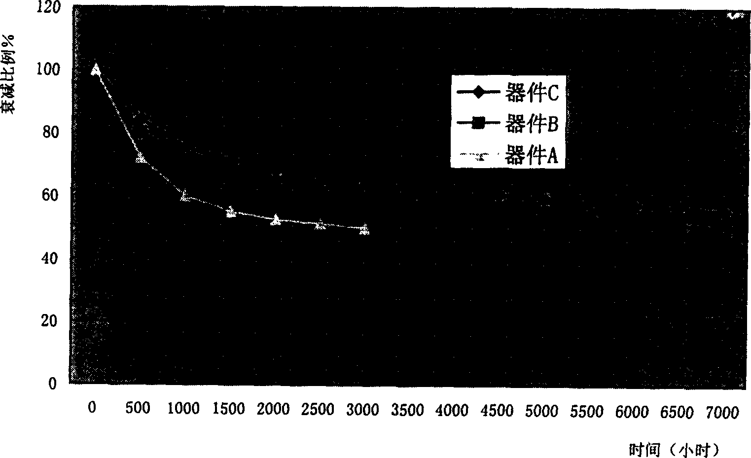
Image

Examples
Embodiment Construction
[0011] Select an ITO glass substrate with a thickness of 200 mm × 200 mm × 0.7 mm for cleaning to remove impurities on the substrate. And use photolithography technology to make the required lattice pattern, including photolithography auxiliary metal electrode, photolithography transparent electrode ITO, photolithography insulating layer, photolithography cathode isolation column layer.
[0012] In the dedicated OLED coating equipment, first use O 2 Plasma or ultraviolet light ozone activates the ITO surface, and then in a high vacuum (vacuum degree above 1×10⁻⁴ Pa) cavity, use physical vapor deposition method to thermally evaporate organic materials, first deposit 60 nanometers thick hole transport material (Sometimes the hole transport layer is divided into two layers, i.e., the hole injection layer and the hole transport layer), and then the light-emitting layer is deposited, using the mixed deposition method, the host H is doped with two or more than two kinds of guest D, ...
PUM
 Abstract
Description
Claims
Application Information