Laser annealing apparatus and annealing method

A laser annealing and laser technology, used in laser welding equipment, chemical instruments and methods, self-area melting methods, etc., can solve the problems of large energy loss, narrow energy condition range, silicon film damage, etc., to achieve excellent performance, mobility high effect

Inactive Publication Date: 2005-08-03
HITACHI DISPLAYS +1
View PDF2 Cites 10 Cited by
  • Summary
  • Abstract
  • Description
  • Claims
  • Application Information

AI Technical Summary

Problems solved by technology

[0005] In order to shape solid-state lasers such as the second harmonic of the continuous oscillation YAG laser used in the above-mentioned prior art into a slender shape, a multi-lens array or kaleidoscope with a complex structure, or rotational diffusion to reduce coherence (coherence) is used The plate acts as a homogenizer (beam shaper), so the energy loss is large
[0006] In addition, the short direction of the laser beam is shaped into a slender shape of about 20 microns, and the desired area is irradiated at a scanning speed of about 100 mm / s. However, the range of energy conditions for obtaining good laterally grown crystals is narrow, and energy fluctuations are easy to occur. damage to the silicon membrane

Method used


Image

  • Laser annealing apparatus and annealing method
  • Laser annealing apparatus and annealing method
  • Laser annealing apparatus and annealing method

Examples


Embodiment Construction

[0025] The present invention will be described in detail below with reference to the drawings of the embodiments.

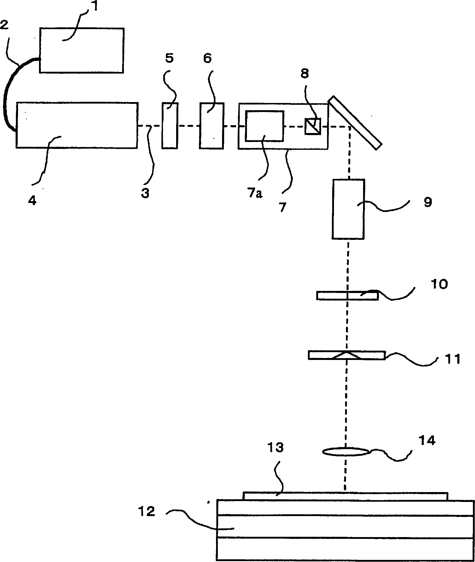
[0026] figure 1 is an optical structure diagram of a laser annealing device according to an embodiment of the present invention. The optical structure is composed of the following components: a laser oscillator 4 that is connected to an excitation LD (laser diode) 1 and an optical fiber 2 to generate a continuous oscillating laser 3, a shutter 5 for turning on / off the laser 3, and a shutter for adjusting the laser 3. An ND filter 6 with continuously variable energy transmittance, a modulator 7 for time-modulating the laser 3 output from the laser oscillator 4 to realize pulsed and time-modulated energy, and a beam for adjusting the laser 3 The beam expander (beam reducer) 9 of the diameter, the beam shaper 10 that the laser 3 is shaped into a slender shape such as a line, a rectangle, an ellipse, and an oblong beam, is used to shape the beam of the laser 3 The ...


PUM

PropertyMeasurementUnit
sizeaaaaaaaaaa
thicknessaaaaaaaaaa

Abstract

When a laser bean temporally modulated in amplitude by a modulator is shaped into a long and narrow beam by a beam shaper, the scanning-direction size of the long and narrow beam shaped by the beam shaper is selected to be in a range of from 2 to 10 microns, preferably in a range of from 2 to 4 microns and the scanning speed of the beam is selected to be in a range of from 300 to 1000 mm / s, preferably in a range of from 500 to 1000 m / s. As a result, damage of the silicon thin film can be suppressed while energy utilizing efficiency of the laser beam can be improved. Accordingly, laterally grown crystals (belt-like crystals) improved in throughput can be obtained on a required region of a substrate scanned and irradiated with the laser beam.

Description

technical field [0001] The present invention relates to a laser annealing method and a laser annealing device suitable for irradiating laser light on an amorphous semiconductor film or a polycrystalline semiconductor film formed on an insulating substrate to improve film quality, expand crystal grains, or perform single crystallization. Background technique [0002] Currently, display devices such as liquid crystal display devices and organic EL display devices form images by switching pixel transistors (thin film transistors) formed of an amorphous or polysilicon film on a substrate such as glass or fused silica. If it is possible to simultaneously form a driver circuit for driving pixel transistors on this substrate, it is possible to drastically reduce manufacturing costs and improve reliability. However, when the silicon film forming the active layer of the transistor (thin-film transistor) constituting the driver circuit is amorphous, the performance of the thin-film tr...

Claims


Application Information

Patent Timeline
Patent Type & Authority Applications(China)
IPC IPC(8): H01L21/324B23K26/073C30B13/24C30B29/06H01L21/20H01L21/268H01L29/04H01L29/786
CPCB23K26/0738H01L29/78675C30B13/24C30B29/06H01L21/2026H01L29/04H01L21/02683H01L21/02422H01L21/02678H01L21/02532H01L21/02691H01L21/324H01L21/20
Inventor 本乡干雄矢崎秋夫波多野睦子野田刚史高崎幸男
Owner HITACHI DISPLAYS
Why Eureka
Try Eureka