Nondestructive testing method for every layer thin film thickness of SAW device with multilayer film structure

A measurement method and technology of film thickness, applied in the direction of electric/magnetic thickness measurement, measuring device, electromagnetic measuring device, etc., can solve the problem of non-destructive and accurate measurement of film thickness, difficulty in determining the value of relative permittivity ε, and large difference in film ε and other issues, to achieve the effect of low cost, improved performance, and simple measurement method

Inactive Publication Date: 2005-09-28
TIANJIN UNIVERSITY OF TECHNOLOGY
View PDF0 Cites 23 Cited by
  • Summary
  • Abstract
  • Description
  • Claims
  • Application Information

AI Technical Summary

Problems solved by technology

However, the ε of films prepared by various artificial growth methods (due to different methods and processes) varies greatly, and it is difficult to determine the exact value of the relative permittivity ε
The ε value of a thin film material prepared by a certain process cannot be used as the relat

Method used


Image

  • Nondestructive testing method for every layer thin film thickness of SAW device with multilayer film structure
  • Nondestructive testing method for every layer thin film thickness of SAW device with multilayer film structure
  • Nondestructive testing method for every layer thin film thickness of SAW device with multilayer film structure

Examples


Embodiment Construction

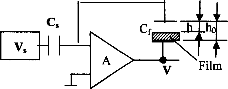
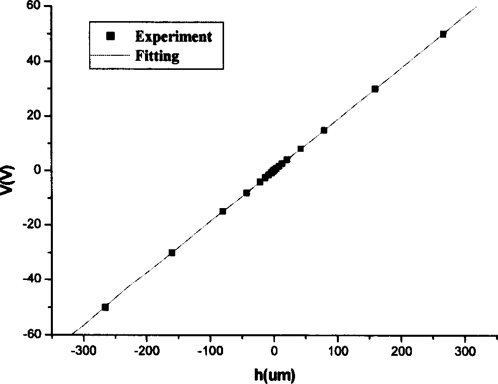
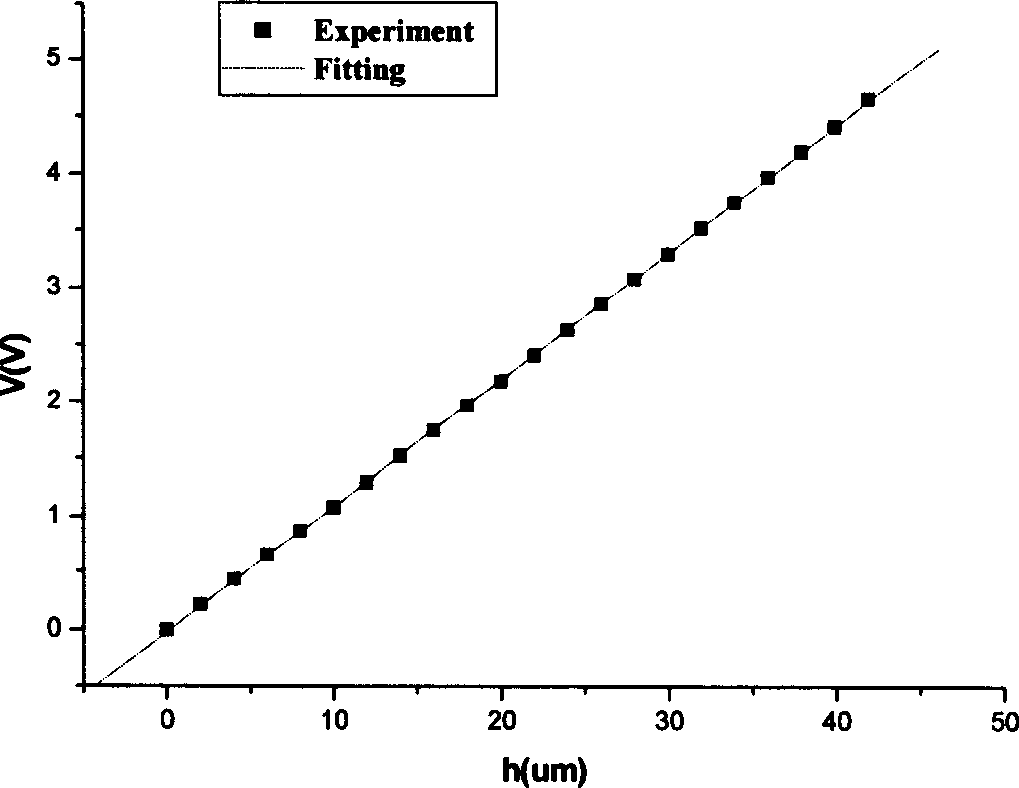
[0028] The present invention utilizes the upper and lower plate electrodes of the parallel plate capacitance micrometer to measure the variation between the two electrodes to measure the thickness of the sample film. The principle diagram is shown in figure 1 .

[0029] In the figure, A is an operational amplifier (Operational Amplifier), Vs is the square wave excitation oscillator signal source voltage, Cs is the standard capacitance (1pF), h is the upper and lower plate sensing capacitance C f The air gap between, V is the amplifier output voltage. The relationship between the operational capacitance sensor and the air gap h is as follows:

[0030] V = - ( C s V s ϵϵ 0 S ) h...


PUM


Abstract

The present invention is non-destructive film thickness measuring method for multilayer film structure in SAW device. The measuring method includes first determination of measurement coefficient k of the measured film sample, subsequent measurement of the total thickness h of the measured film sample, and final calculation of thickness of the measured film based on the formula hfilm=hsubstrate-hsample. The measuring method of the present invention is based on parallel plate capacitor micro measurement principle and has measurement precision up to 1 nm. The method is simple non-contact measurement with low cost and is suitable for the measurement film thickness and film parallelism of various kinds of multilayer film structure.

Description

【Technical field】 [0001] The invention relates to the field of thin-film electronic devices, in particular to a method for nondestructively measuring the thickness of each layer of a multi-layer film structure SAW device. 【technical background】 [0002] In recent years, multilayer film structure electronic devices have become an important part of emerging interdisciplinary disciplines and emerging industries such as microelectronics, optoelectronics, magnetoelectronics, and sensors. With the development of electronic thin film science and technology, various thin film materials, especially multi-layer film structure materials, are constantly emerging. The characterization of the thickness, morphology and structure of thin film materials has become a common concern in thin film preparation and application. In particular, the film thickness of a multilayer SAW device is a very important parameter. Non-destructive and accurate measurement of the film thickness of each layer is ...

Claims


Application Information

Patent Timeline
IPC IPC(8): G01B7/06G01B21/08
Inventor 杨保和陈希明吴小国马靖
Owner TIANJIN UNIVERSITY OF TECHNOLOGY
Why Eureka
Try Eureka