Large area internal series dye sensitization nano thin film solar cell and producing method thereof

A technology of internal series connection and solar cells, applied in circuits, photovoltaic power generation, electrical components, etc., can solve stability problems, difficult material selection and other problems, achieve high output voltage, overcome technical difficulties and material selection difficulties, and avoid stability Problems and Effects of Industrialization Technology Problems

Inactive Publication Date: 2005-09-28
铜陵中科聚鑫太阳能有限责任公司
View PDF0 Cites 12 Cited by
  • Summary
  • Abstract
  • Description
  • Claims
  • Application Information

AI Technical Summary

Problems solved by technology

[0007] This method can be used to prepare large-area internal series dye-sensitized nano-thin film solar cells, overcome the technical difficulties and material selection difficulties brought about by preparing large-area dye-sensitized nano-thin film solar cell

Method used


Image

  • Large area internal series dye sensitization nano thin film solar cell and producing method thereof
  • Large area internal series dye sensitization nano thin film solar cell and producing method thereof
  • Large area internal series dye sensitization nano thin film solar cell and producing method thereof

Examples


Embodiment 1

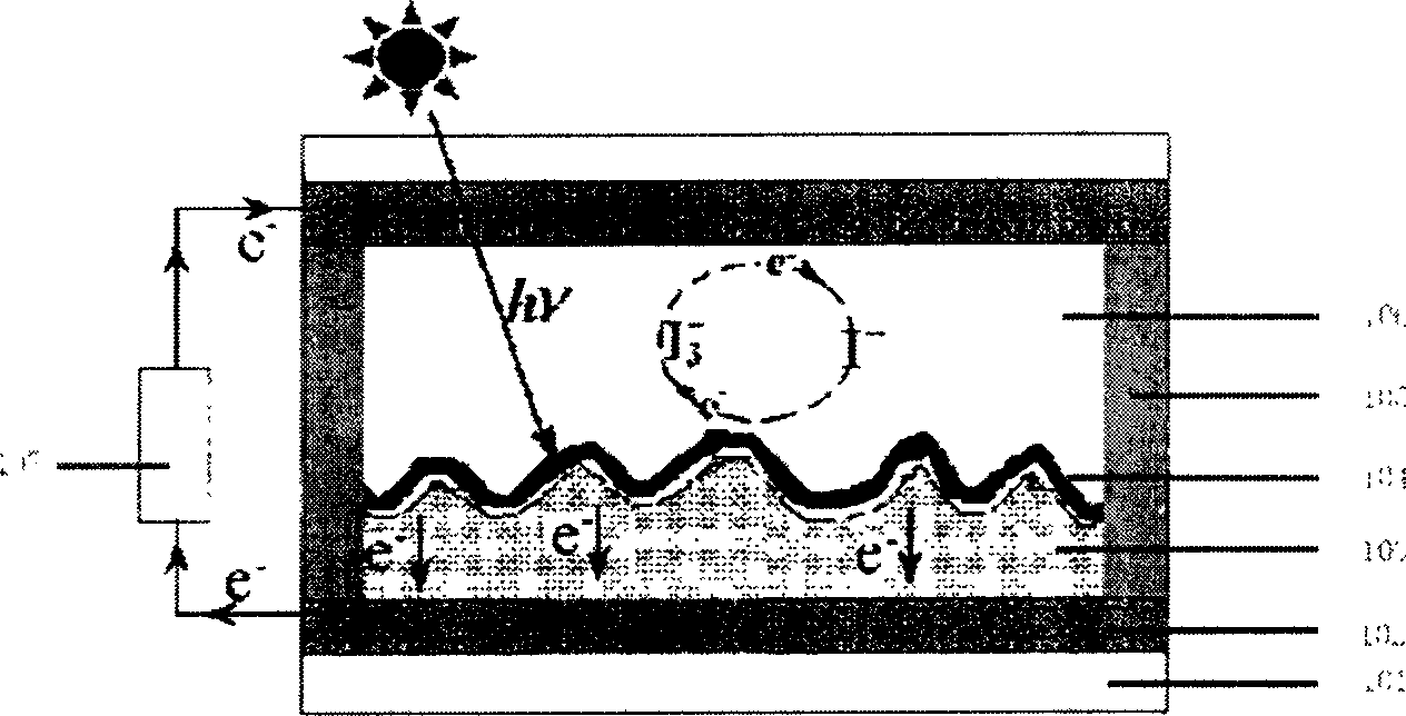
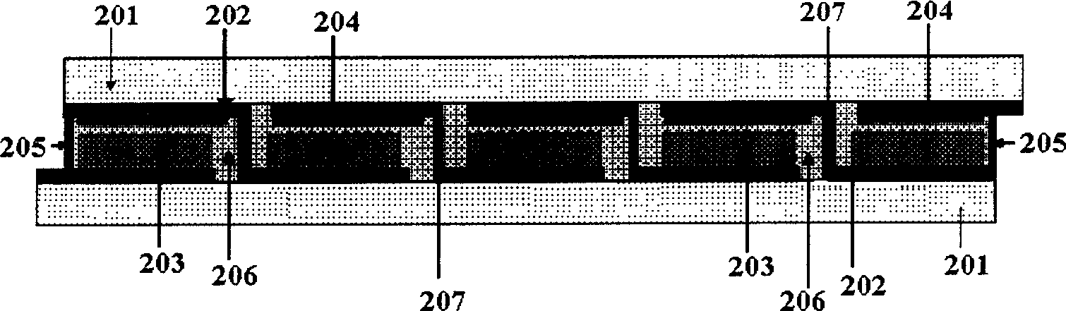
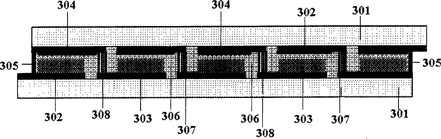
[0038] see figure 1 , image 3 .

[0039] 1. Preparation of transparent conductive electrode material: Put a transparent substrate 301, such as: transparent conductive glass, or conductive plastic, or transparent conductive polymer material, on it to cover a layer of conductive film 302, use laser marking, or other mechanical engraving Divide the conductive film 302 on the conductive glass into certain sizes according to design requirements by scratching or high-pressure water marking, and clean it for later use.

[0040] 2. Preparation of photoanode (negative electrode): On conductive glass 301, methods such as printing, or spraying, or sputtering prepare nanometer (or porous) film 303 (such as nanometer TiO 2 Porous film, or nano ZnO porous film), the thickness of the film can be between 0.1 micron and 1 mm, and it is sintered and processed according to the characteristics of the material itself (such as: to prepare a battery with a transparent conductive glass as a substr...

Embodiment 2

[0046] see figure 2 . Put the photoanode printed with nanoporous film into the dye solution for more than one hour, so that the dye can be evenly adsorbed in the porous semiconductor film, and you can choose to use a specific solution to wash it, so that there is no dye adsorption in the place where there is no film. Take 100 grams of 200-mesh titanium powder, 30 grams of silica gel and 0.1 grams of Platium-Divinyltetramethyl-Disiloxrane Complex, mix them evenly as electrode materials, and print sealing paste outside the electrode materials. The rest are the same as example 1.


PUM

PropertyMeasurementUnit
Thicknessaaaaaaaaaa
Thicknessaaaaaaaaaa

Abstract

A film solar cell comprises top and bottom transparent baseboards. It is prepared by sealing baseboard periphery to form cavity with electrolyte, arranging transparent conduction film in interval on substrate, making conduction film on one substrate have catalyst layer and conduction film on another one have nanomultihole semiconductor material block, soaking dyestuff in said nanomaterial and connecting two staggered transparent conduction films by series electrodes. The internal series electrode is also prepared for obtaining output current of solar cell.

Description

technical field [0001] The invention relates to the fields of semiconductor materials, macromolecular materials, organic materials, inorganic materials, renewable energy sources and solar cells, in particular to a large-area internal series dye-sensitized nano-film solar cell and a manufacturing method thereof. technical background [0002] In 1991, the laboratory of Professor M.Grtzel of the Institute of Technology in Lausanne, Switzerland reported a new dye-sensitized nano-thin film solar cell on Nature (O'Regan, B.; Grtzel.M, 1991, 353, 737). The research results immediately received widespread international attention and attention. Since 1991, it has been an international research hotspot. Its low cost and production cost, easy industrial production technology, and broad application prospects have attracted many scientists and enterprises to invest. [0003] Dye-sensitized nano-thin-film solar cells use organic photosensitive functional molecules combined with semi-s...

Claims


Application Information

Patent Timeline
IPC IPC(8): H01L31/04H01M14/00
CPCY02E10/542
Inventor 戴松元王孔嘉翁坚陈双宏
Owner 铜陵中科聚鑫太阳能有限责任公司
Why Eureka
Try Eureka