Process for making tripolar carbon nanotube field emission display having self-aligning technique

A self-alignment process, carbon nanotube technology, applied in the manufacture of discharge tubes/lamps, cold cathode manufacture, electrode system manufacture, etc. and carbon nanotube cathode strip alignment errors, to achieve the effect of simplifying the device fabrication process steps, good field emission capability, and shortening the device fabrication cycle

Inactive Publication Date: 2005-11-23
ZHONGYUAN ENGINEERING COLLEGE
View PDF0 Cites 26 Cited by
  • Summary
  • Abstract
  • Description
  • Claims
  • Application Information

AI Technical Summary

Problems solved by technology

In the device manufacturing process of flat-panel devices, limited by the actual process manufacturing accuracy and actual equipment level, there is always a certain alignment error between the preparation of carbon nanotube cathode strips and the cathode conductive strips, while the control grid strips and There is also a certain alignment error between the carbon nanotube cathode strips
On the one hand, although these can be controlled within the allowable range in actual device fabrication, how can we minimize the negative impact of alignment errors and produce devices with higher precision and better field emission performance? On the other hand, in the manufacturing process of large-area devices, once there is an alignment error in a certain part of the device, it will cause the failure of the overall device. For example: due to alignment errors, a certain The control grid bar and the carbon nanotube cathode bar are connected to each other, so that the control grid cannot effectively control the carbon nanotube cathode; due to misalignment, there is only A small number of parts overlap, so that only a small part of the carbon nanotube cathode can be applied with voltage, and most of the carbon nanotube cathode is in a floating state, which not only wastes a lot of carbon nanotube cathode materials, but also improves the field emission performance of the device. A sharp decrease, etc., will result in a very low device manufacturing success rate, and the device manufacturing cost will be greatly increased, which is contrary to the requirement to reduce the device manufacturing cost as much as possible
In addition, in the process of device manufacturing, the accuracy requirements of equipment and manufacturing process will be correspondingly improved, which will further increase the manufacturing cost of devices virtually.
For how to effectively and fully utilize the good field emission characteristics of grown carbon nanotube cathodes, avoid the influence of other processes on carbon nanotube cathodes, and at the same time simplify the device manufacturing process, improve the success rate of device manufacturing, and reduce device manufacturing costs , so that the manufacturing process of the overall device tends to be simplified, reducing the material requirements for making device materials. At present, there is no effective solution

Method used


Image

  • Process for making tripolar carbon nanotube field emission display having self-aligning technique
  • Process for making tripolar carbon nanotube field emission display having self-aligning technique
  • Process for making tripolar carbon nanotube field emission display having self-aligning technique

Examples


Embodiment Construction

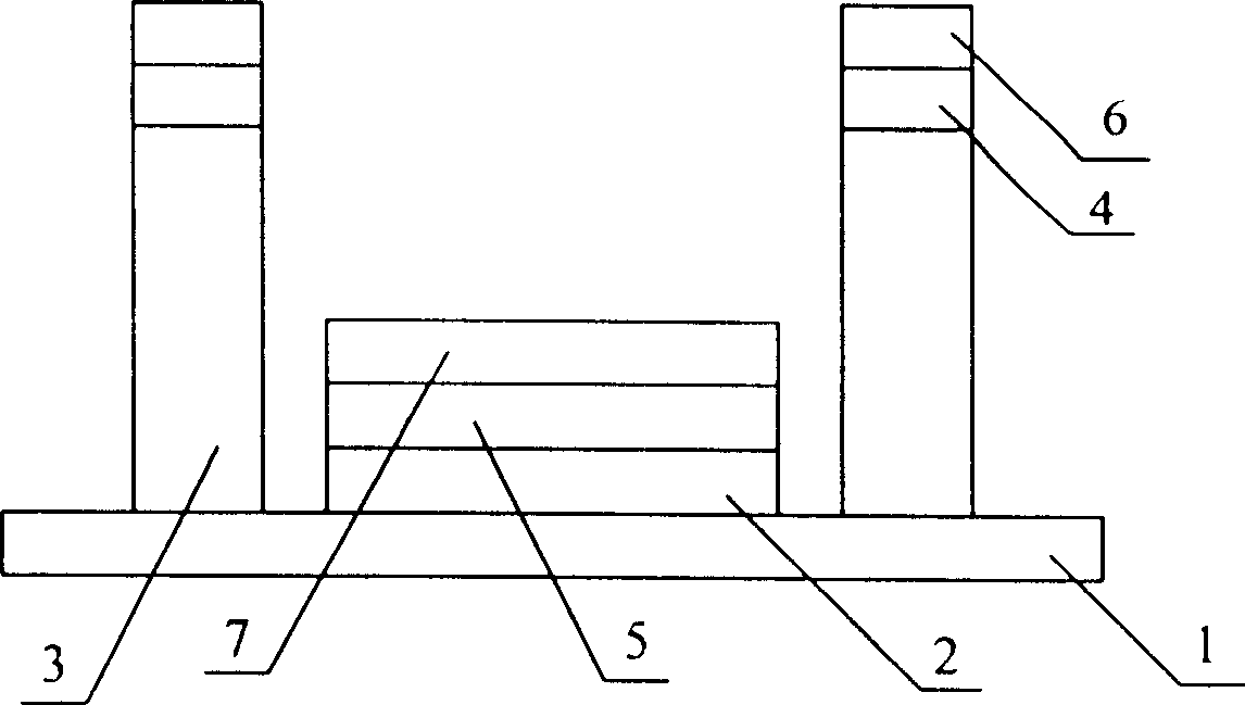
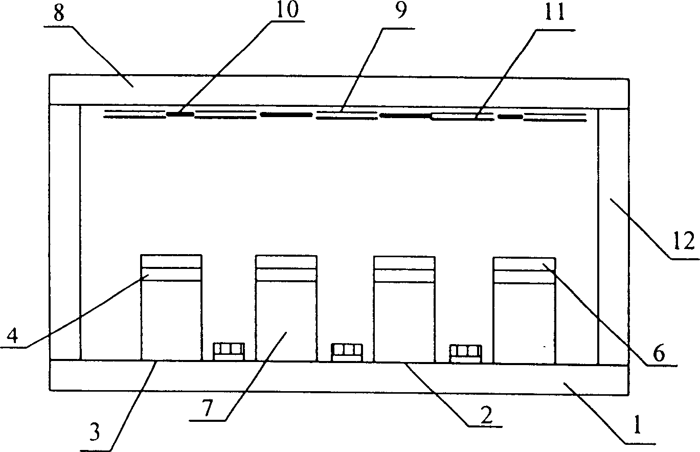
[0031] Such as figure 1 , 2 , 3, the present invention will be further described below in conjunction with the accompanying drawings and embodiments, but the present invention is not limited to these embodiments.

[0032] The manufacturing process of the triode structure carbon nanotube field emission display with self-alignment process is as follows:

[0033] 1. Scribing of the cathode substrate glass (1): Scribing the whole flat glass,

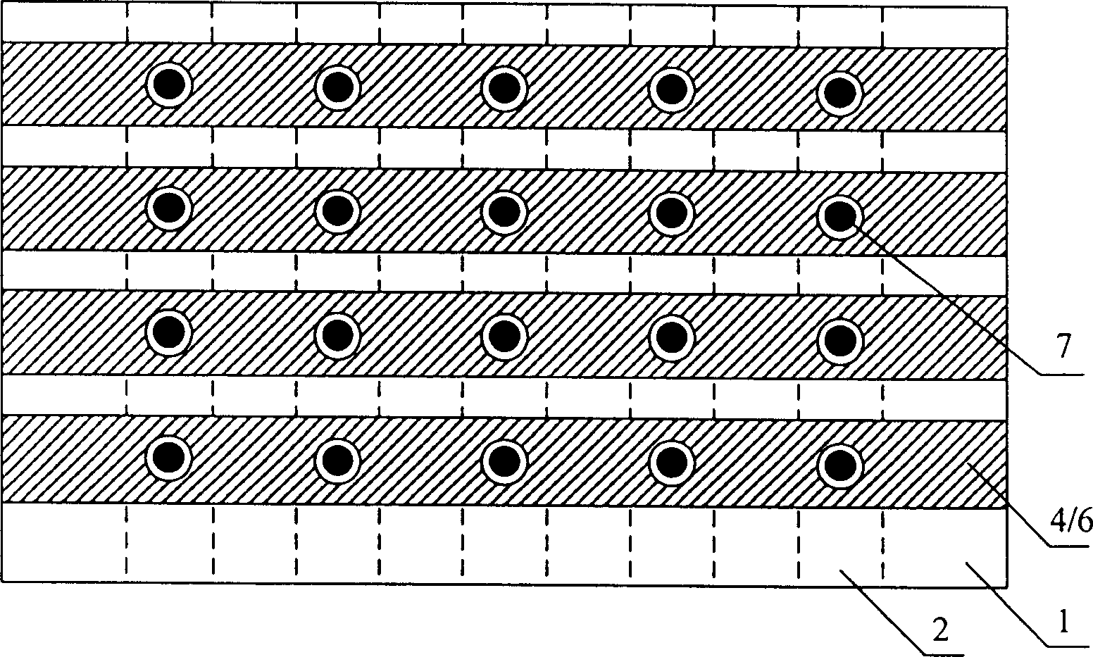
[0034] 2. Production of the cathode conductive strip (2):

[0035] Evaporating a layer of tin indium oxide thin film layer on the cathode base glass (1); performing photoetching on the evaporated tin indium oxide thin film layer to form cathode conductive strips (2);

[0036] 3. Growth of insulating layer (3):

[0037] A silicon dioxide layer is fabricated on the cathode substrate glass (1) to be used as an insulating layer (3) between the control grid and the carbon nanotube cathode;

[0038] 4. Photolithography of the insulating layer...


PUM


Abstract

This invention relates to carbon nanometer tube negative electrode structure eradiation display device, wherein, the display comprises negative panel, positive panel and glass closure frame formed sealed vacuum chamber, wherein, the positive panel is grown with carbon nanometer negative electrode located on the top of the negative electrode to control the electron eradiation control grid electrode and adopts self-aligning process.

Description

technical field [0001] The invention belongs to the fields of vacuum science and technology, nano science and technology and microelectronics science and technology, and relates to the production of devices for flat panel displays, in particular to the content of the production of devices for field emission displays with carbon nanotube cathodes, in particular to A field emission display of carbon nanotubes with a self-alignment process and its manufacturing process. Background technique [0002] At present, for the field emission flat panel display devices manufactured by using carbon nanotubes as cathode materials, the cathode manufacturing processes are various and different. The field emission characteristics of carbon nanotube cathodes prepared by the growth process are better than those of carbon nanotube cathodes prepared by other transplantation methods, but are limited by the characteristics of other structural manufacturing processes of the device, such as the gate...

Claims


Application Information

Patent Timeline
IPC IPC(8): H01J9/02
Inventor 李玉魁高宝宁刘兴辉
Owner ZHONGYUAN ENGINEERING COLLEGE
Why Eureka
Try Eureka