Manufacturing method of solid-state plasma diode for preparing holographic antenna

A manufacturing method, holographic antenna technology, applied in semiconductor/solid-state device manufacturing, antenna, antenna parts, etc., to achieve good device performance

Inactive Publication Date: 2017-05-10
XIAN CREATION KEJI CO LTD
View PDF7 Cites 0 Cited by
  • Summary
  • Abstract
  • Description
  • Claims
  • Application Information

AI Technical Summary

Problems solved by technology

[0004] However, most of the current research is limited to gaseous plasma

Method used


Image

  • Manufacturing method of solid-state plasma diode for preparing holographic antenna
  • Manufacturing method of solid-state plasma diode for preparing holographic antenna
  • Manufacturing method of solid-state plasma diode for preparing holographic antenna

Examples


Example Embodiment

[0056] Embodiment one

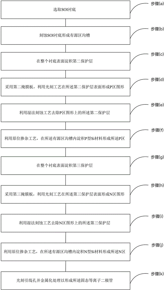
[0057] See image 3 , image 3 It is a flowchart of a method for manufacturing a solid-state plasma diode for preparing a holographic antenna according to an embodiment of the present invention. The method is suitable for preparing a lateral solid-state plasma diode based on SOI, and the solid-state plasma diode is mainly used for making a holographic antenna. The method comprises the steps of:

[0058] (a) select SOI substrate;

[0059] Among them, for step (a), the reason for using SOI substrate is that solid-state plasma antennas require good microwave characteristics, and solid-state plasma diodes need to have good carriers, that is, solid-state plasmas, in order to meet this requirement. capability, while silicon dioxide (SiO 2 ) can confine carriers, that is, solid-state plasma, in the top layer silicon, so SOI is preferably used as the substrate of solid-state plasma diodes.

[0060] (b) etching the SOI substrate to form trenches in the acti...

Example Embodiment

[0097] Embodiment two

[0098] See Figure 4a-Figure 4r , Figure 4a-Figure 4r It is a schematic diagram of another method of manufacturing a solid-state plasma diode for preparing a holographic antenna according to an embodiment of the present invention; 2 The protective solid-state plasma diode is taken as an example to describe in detail, and the specific steps are as follows:

[0099] S10, selecting an SOI substrate.

[0100] See Figure 4a , the crystal orientation of the SOI substrate 101 is (100), in addition, the doping type of the SOI substrate 101 is p-type, and the doping concentration is 10 14 cm -3 Yes, the thickness of the top Si layer is, for example, 20 μm.

[0101] S20, depositing a layer of silicon nitride on the surface of the SOI substrate.

[0102] See Figure 4b A silicon nitride layer 201 is deposited on the SOI substrate 101 by using a chemical vapor deposition (Chemical vapor deposition, CVD for short) method.

[0103] S30, etching the SOI sub...

Example Embodiment

[0136] Embodiment Three

[0137] Please refer to Figure 5 , Figure 5 It is a schematic diagram of the device structure of another solid-state plasma diode for preparing a holographic antenna according to an embodiment of the present invention. The solid state plasma diode employs the above as image 3 made by the fabrication method shown. Specifically, the solid-state plasma diode is prepared and formed on the SOI substrate 301, and the P region 303, the N region 304, and the i region laterally located between the P region 303 and the N region 304 of the solid-state plasma diode are all located on the SOI substrate. The top Si layer 302 at the bottom.


PUM


Abstract

The invention relates to a manufacturing method of a solid-state plasma diode for preparing a holographic antenna. The manufacturing method comprises the steps of (a) selecting an SOI substrate; (b) etching the SOI substrate to form an active region groove; (c) depositing a P-type Si material and an N-type Si material on the active region groove by adopting an in-situ doping process to form a P region and an N region separately; and (d) photoetching a lead hole and carrying out metallized treatment to form the solid-state plasma diode. The high-performance solid-state plasma diode suitable for forming the holographic antenna can be prepared and provided by using the in-situ doping process.

Description

technical field [0001] The invention relates to the technical field of integrated circuits, in particular to a method for manufacturing a solid-state plasma diode for preparing a holographic antenna. Background technique [0002] Due to its relatively large weight and volume, the traditional metal antenna is inflexible in design and manufacture, and its self-reconfiguration and adaptability are poor, which seriously restricts the development and performance improvement of radar and communication systems. Therefore, in recent years, the theory of antenna broadband, miniaturization, and reconfiguration and multiplexing has become increasingly active. [0003] Against this background, the researchers proposed a new antenna concept-plasma antenna, which is a radio-frequency antenna that uses plasma as a guiding medium for electromagnetic radiation. The plasma antenna can change the instantaneous bandwidth of the antenna by changing the plasma density, and has a large dynamic ra...

Claims


Application Information

Patent Timeline
IPC IPC(8): H01Q1/22H01Q1/36H01L21/329H01L29/868
CPCH01Q1/2283H01L29/6609H01L29/868H01Q1/36
Inventor 尹晓雪张亮
Owner XIAN CREATION KEJI CO LTD
Why Eureka
Try Eureka