Semiconductor device, method for manufacturing same, and power converter using such semiconductor device
A technology of semiconductors and light-emitting semiconductors, applied in semiconductor devices, semiconductor/solid-state device components, circuits, etc., can solve problems such as difficult power semiconductor devices, large uncertain losses, and large total losses
- Summary
- Abstract
- Description
- Claims
- Application Information
AI Technical Summary
Problems solved by technology
Method used
Image
Examples
no. 1 example
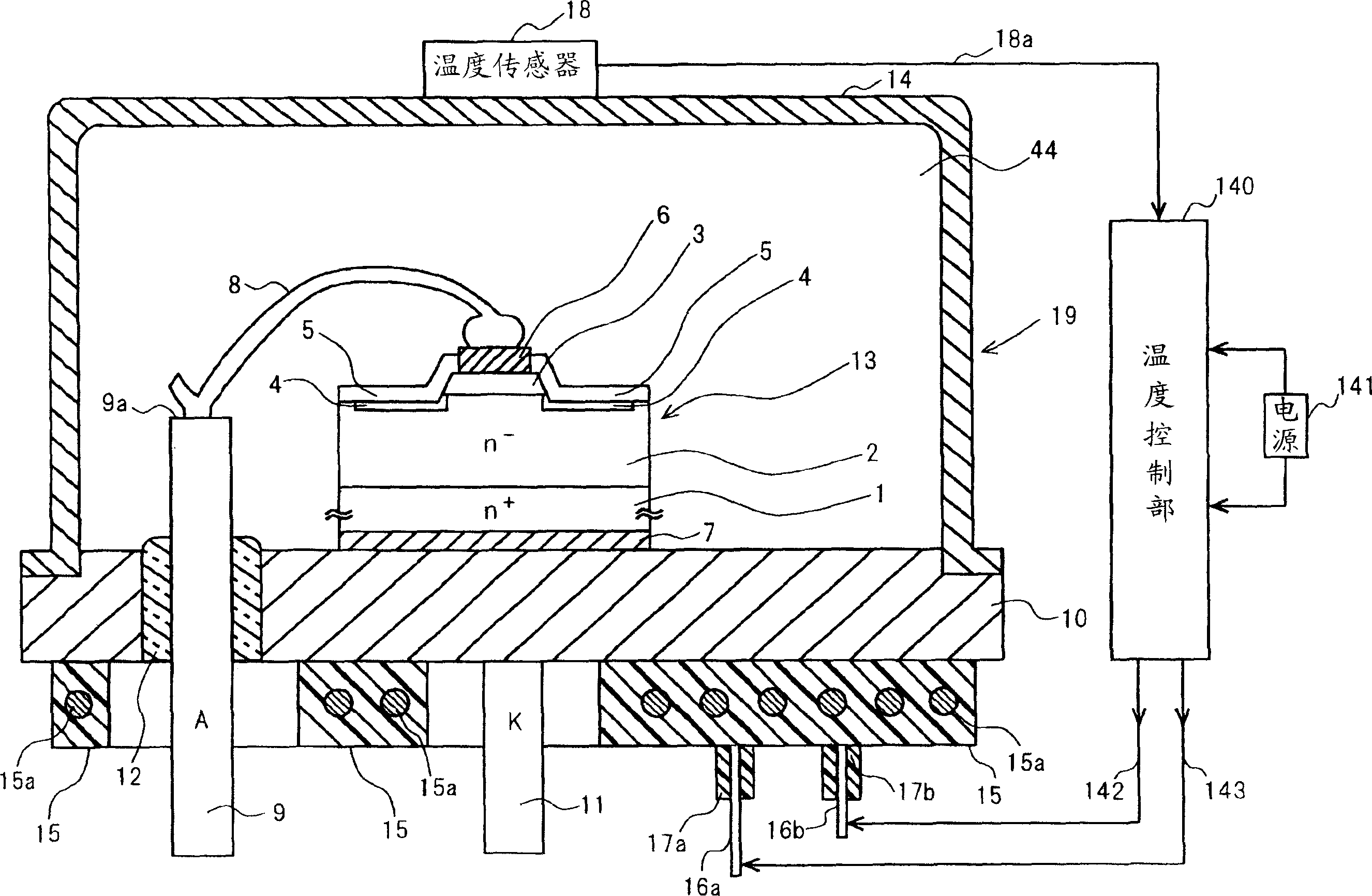
[0046] The semiconductor device of the first embodiment of the present invention is a SiC (silicon carbide) pn diode device 19 with a withstand voltage of 8.5 kV. figure 1 illustrate.
[0047] figure 1 is a cross-sectional view of the SiC-pn diode device 19 of the first embodiment of the present invention. exist figure 1Among them, the pn diode element 13 of SiC is a 4-layer hexagonal element, and a drift layer 2 of n-type SiC with a thickness of about 95 μm and a low impurity concentration of n-type SiC is formed on the cathode region 1 of n-type SiC with a thickness of about 300 μm. . A cathode metal electrode 7 is formed below the cathode region 1 . An anode region 3 of p-type SiC constituting a main bond with the drift layer 2 is formed in the central region of the drift layer 2 . An electric field relaxation region 4 of p-type SiC is formed around the anode region 3 . An anode metal electrode 6 is formed on the anode region 3 . A surface protection film 5 is formed...
no. 2 example
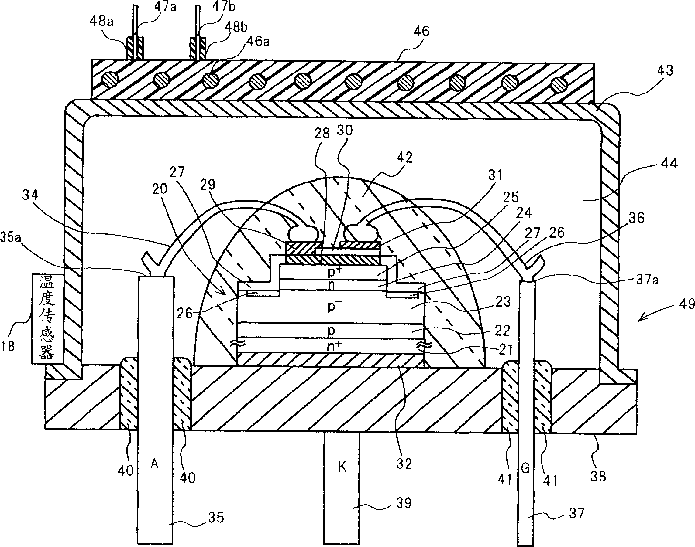
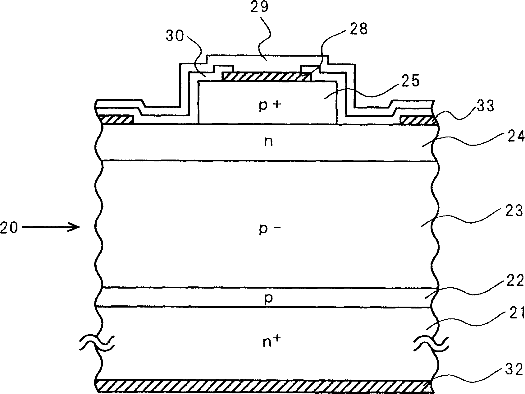
[0058] The semiconductor device of the second embodiment of the present invention is a SiC-GTO thyristor (Gate Turn-Off Thyristor) device 49 with a withstand voltage of 5 kV, figure 2 shows its cross-section. image 3 is said to be figure 2 A sectional view of the unit obtained by cutting the GTO thyristor element 20 in a plane perpendicular to the paper plane. In actual components, image 3 The illustrated units are connected in plurality in the left-right direction of the figure. In addition, in figure 2 middle, image 3 The units shown are connected in multiples in a direction perpendicular to the paper plane of the drawing. exist figure 2 as well as image 3 In the present invention, a buffer layer 22 of p-type SiC having a thickness of about 3 μm is provided on a cathode region 21 of high impurity concentration n-type SiC having a thickness of about 320 μm. A cathode electrode 32 is arranged below the cathode region 21 . A base layer 23 of p-type SiC having a...
no. 3 example
[0071] A semiconductor device according to a third embodiment of the present invention is an optically coupled wide-gap power semiconductor device, and FIG. 4 shows a cross-sectional view thereof. In the figure, a GaN (gallium nitride)-GTO thyristor element 51 with a withstand voltage of 3 kV and a current capacity of 160 A is used as a main power semiconductor element having a light emitting function. A SiC photodiode 52 is used as a light receiving element. A SiC photodiode 52 is provided in the same package facing the GaN-GTO thyristor element 51 .
[0072] In the GaN-GTO thyristor element 51 shown in FIG. 4 , a p-base of p-type GaN with a thickness of about 35 μm and a low impurity concentration is provided on the cathode region 51 a of n-type GaN with a thickness of about 250 μm and a high impurity concentration. polar region 53 . An n-base region 54 of high impurity concentration n-type GaN having a thickness of about 1.7 μm is formed in the central region of the p-bas...
PUM
 Abstract
Description
Claims
Application Information


