
Method for raising semiconductor laser yield

A technology of lasers and yield rate, applied in semiconductor lasers, lasers, laser components, etc., can solve problems such as increased production costs, laser damage, poor airtightness, etc., to save costs, avoid waste, improve reliability and The effect of yield

Active Publication Date: 2005-12-21
WUHAN TELECOMM DEVICES
View PDF0 Cites 9 Cited by
  • Summary
  • Abstract
  • Description
  • Claims
  • Application Information

AI Technical Summary

Problems solved by technology

For these lasers, the power stability of most lasers can meet the requirements of qualified products after rework such as lid opening displacement correction; however, the one-time yield of the device cannot be improved.
Even if unqualified devices are uncapped and adjusted to be qualified, the consequences will be to prolong the production cycle of the devices, increase production costs, and also bring new quality risks such as poor airtightness after resealing.
There are also some laser components that leave the factory without going through the elimination process of high and low temperature cycles at all. On the surface, the yield rate is relatively high, but these lasers have not been completely released due to internal stress. Displacement occurs, resulting in a reduction in the fiber output power of the laser, and the reliability cannot be effectively guaranteed, which will bring huge losses to device manufacturers and system manufacturers
[0006] 2. The inherent defects of the laser chip itself lead to low reliability of the laser, such as defects in the material growth process of the epitaxial wafer or in the post-production process of the epitaxial wafer or certain damage areas of the laser

Method used


Image

  • Method for raising semiconductor laser yield
  • Method for raising semiconductor laser yield

Examples


Embodiment Construction

[0041] 1. The best state of the relevant steps

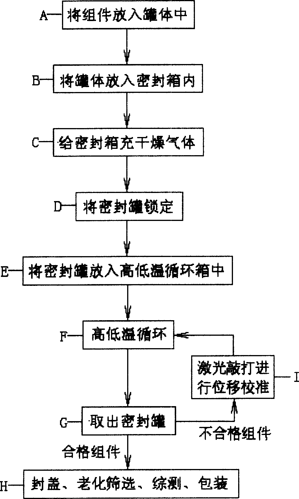
[0042] Step ③ Fill the sealed box with dry gas C for 30 minutes.

[0043] Step ④ lock the sealed tank D, the oxygen content in the sealed box is 20%, and the water vapor content is 5000ppm.

[0044] Step ⑥ high and low temperature cycle F, the set time of each cycle is 2 hours.

[0045] Step ⑦ Take out the sealed tank G, after completing 20 high and low temperature cycles as described in step ⑥, when the temperature in the circulation box is 25°C, take out the sealed tank 1 from the circulation box.

[0046] 2. The structure of the sealed tank 1

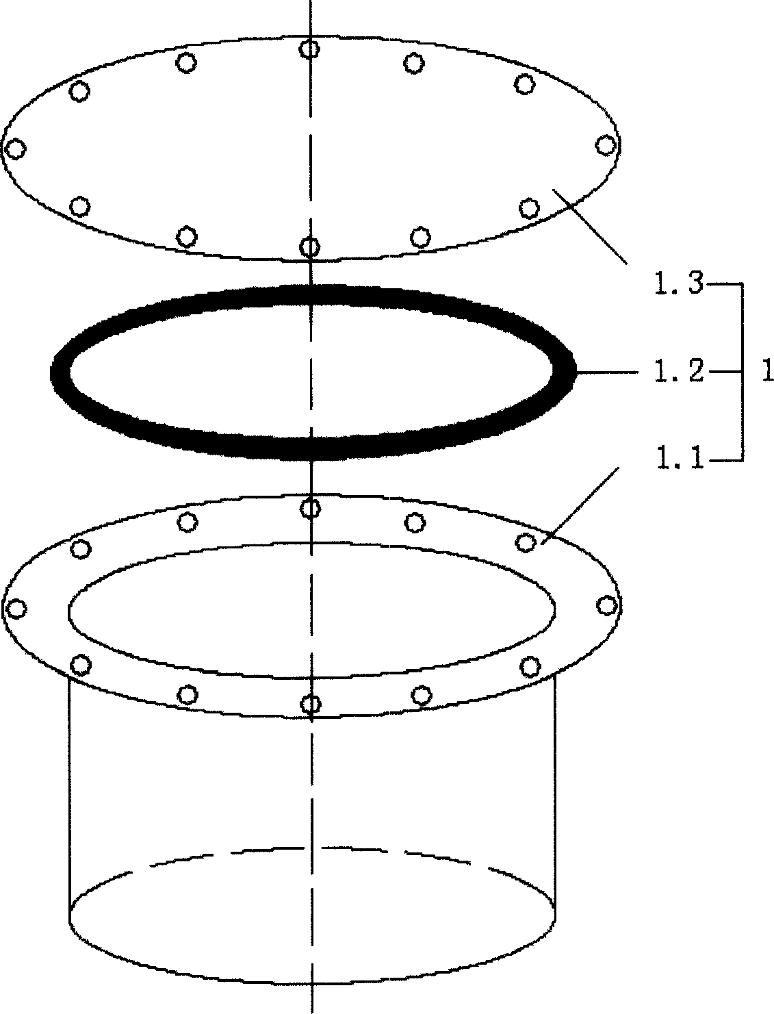
[0047] Such as figure 1 The sealed tank 1 is composed of a tank body 1.1, a tank cover 1.2 and a sealing ring 1.3; a sealing ring 1.3 is arranged between the tank body 1.1 and the tank cover 1.2, and is fixed by screws.

[0048] Described tank body 1.1, its structure is a kind of metal container that has edge, is evenly distributed with the small hole that is used for connecting on...


PUM


Abstract

The invention is related to modifying technique for packaging semiconductor laser. Other packaging steps finished and not closed over laser modules are put into airtight container with good heat-conducting property to carry out high and low temperature cycle. After residual stress is released fully, fine adjustment is carried out for coupling welded support in light power changed modules through laser beat etc. technique to make their light power get back to level before high and low temperature cycle. Then, steps including closing over, burn in screen, testing, packaging are carried out for the modules, which are through the said laser beat, passed high and low temperature cycle again and unchanged light power, so as to obtain high reliable semiconductor laser in high yield. The invention prevents wasting material and working hours, and saves cost.

Description

technical field [0001] The invention relates to a method for improving the yield of semiconductor lasers in the field of semiconductor optoelectronics technology, in particular to an improvement of the packaging process of semiconductor lasers, especially the improvement of the packaging process of high-power semiconductor lasers with pigtails. Background technique [0002] Low cost and high reliability are the basic requirements put forward by the development of optical communication technology for semiconductor lasers. Improving the yield of lasers on the basis of ensuring reliability is an effective way to reduce production costs. Therefore, how to improve the reliability and yield of lasers is especially important. [0003] There are many factors that affect the reliability and yield of lasers, and there are the following two types in combination: [0004] 1. In the laser packaging process, due to the mismatch of physical parameters of various component materials, there...

Claims


Application Information

Patent Timeline
IPC IPC(8): H01S5/022
Inventor 李明徐顺川林雪枫
Owner WUHAN TELECOMM DEVICES
Learn More