Buffering layer of ternary nitride for nitride luminescent assembly and its production

A technology of ternary nitride and light-emitting components, which is applied in the direction of electrical components, semiconductor devices, circuits, etc., can solve the problems of inability to effectively reduce dislocation density, reduce production efficiency, and increase difficulty, so as to simplify the heating and cooling process and time , Improve control and simplify process complexity

Active Publication Date: 2005-12-28
EPISTAR CORP
View PDF0 Cites 4 Cited by
  • Summary
  • Abstract
  • Description
  • Claims
  • Application Information

AI Technical Summary

Problems solved by technology

[0003] Most of the traditional nitride components form an AlGaInN series nitride buffer layer on a sapphire substrate, and then perform a nitride epitaxy process on this buffer layer; due to the problem of lattice constant matching, even up to now, it is still unable to effectively reduce dislocations Density; it is generally believed that the density of dislocations has a considerable relationship with the quality of components. In order to improve the quality of nitride growth, the traditional nitride epitaxy process uses two-step growth, that is, at low temperature (500 ~ GaN at 600°C) is used as a buffer layer, and then undergoes a specific heating process and high temperature (1000-1200°C) treatment to crystallize (Crystallization), and then continue the epitaxial growth of each epitaxial stack
Since the quality of the buffer layer directly affects the subsequent epitaxial quality, hundreds of epitaxial parameters such as the thickness and temperature of the buffer layer, the recovery and recrystallization process of heating, the ratio and flow rate of various reaction gas flows must be carefully controlled, resulting in The complexity and difficulty of the process increase, coupled with the need to increase the growth temperature, low temperature switching, the time-consuming heating and cooling process and waiting for the temperature to stabilize, which virtually reduces the production efficiency

Method used


Image

  • Buffering layer of ternary nitride for nitride luminescent assembly and its production
  • Buffering layer of ternary nitride for nitride luminescent assembly and its production
  • Buffering layer of ternary nitride for nitride luminescent assembly and its production

Examples


Embodiment 1

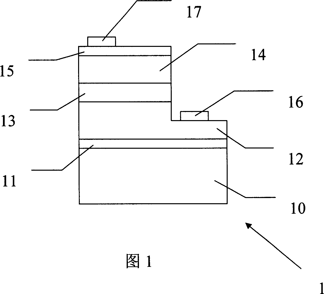
[0030] Please refer to FIG. 1, according to a preferred embodiment of the present invention, it is a nitride light-emitting component 1 with an aluminum gallium nitride (AlGaN) buffer layer, including a sapphire substrate 10; an aluminum gallium nitride buffer layer formed on the sapphire substrate 11. An N-type nitride semiconductor stack 12 formed on the aluminum gallium nitride buffer layer 11, wherein the surface of the N-type nitride semiconductor stack 12 away from the substrate 10 includes an epitaxial region 121 and an N-type electrode contact region 122; The gallium nitride / indium gallium nitride multiple quantum well light-emitting layer 13 formed on the epitaxial region 121; the P-type nitride semiconductor stack 14 formed on the nitride multiple quantum well light-emitting layer 13; formed on the P The metal transparent conductive layer 15 on the nitride semiconductor lamination layer 14; the N-type electrode 16 formed on the N-type electrode contact region 122; and...

Embodiment 2

[0033] Another preferred embodiment of the present invention is a nitride light-emitting component 2 with an aluminum gallium nitride (AlGaN) buffer layer. Its component structure is similar to that of embodiment 1, only the material and manufacturing method of the buffer layer are different. The formation steps of the aluminum gallium nitride buffer layer are as follows:

[0034] The organoaluminum reaction source TMAl is introduced at 1020°C to form an aluminum-rich transition layer; the organic gallium reaction source TMGa and the nitrogen reaction source NH are introduced at the same temperature 3 , to directly grow high-temperature gallium nitride stacks; during this period, the aluminum atoms in the aluminum-rich transition layer will diffuse upwards, and the nitrogen atoms and gallium atoms above it will also diffuse downwards to bond with the aforementioned aluminum atoms and rearrange them, thereby forming AlGaN buffer layer.

[0035] In the nitride light-emitting de...

Embodiment 3

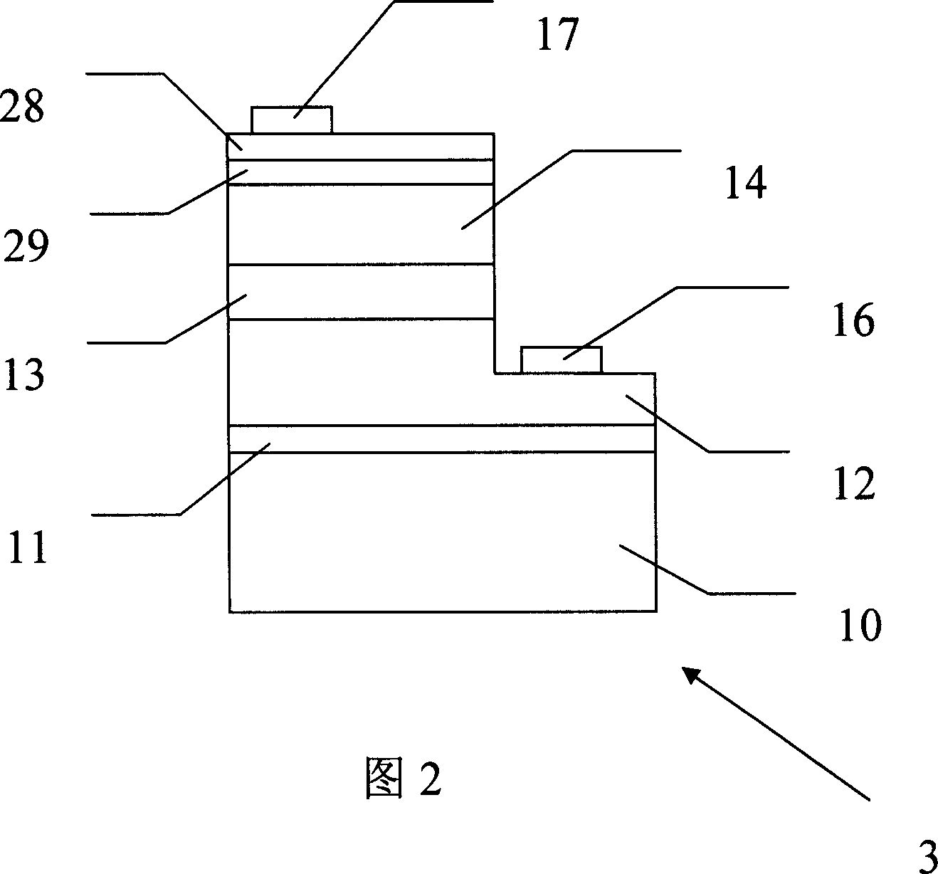
[0037] Please refer to FIG. 3 , according to another preferred embodiment of the present invention, a nitride light-emitting component 3 with an aluminum gallium nitride (AlGaN) buffer layer, and a nitride light-emitting component with an aluminum gallium nitride (AlGaN) buffer layer The difference between 1 and 2 is that the metal transparent conductive layer on the P-type nitride semiconductor layer 14 is replaced by a transparent oxide conductive layer 28, and a high concentration of N is formed between the P-type nitride semiconductor layer 14 and the transparent oxide conductive layer 28. Type reverse tunnel contact layer 29, its thickness is less than 10nm, and its carrier concentration is higher than 1×10 19 cm -3 above. Since the transparent oxidized conductive layer 28 and the P-type nitride semiconductor layer 14 are less likely to form a good Ohmic contact, the transparent oxidized conductive layer is formed through the high-concentration N-type reverse tunnel cont...


PUM

PropertyMeasurementUnit
thicknessaaaaaaaaaa
thicknessaaaaaaaaaa

Abstract

The invention consists of the base board, the ternary nitride buffer layer formed on the base board, the first conducting nitride semiconductor layer formed on the ternary nitride buffer layer, the luminescent layer formed on the first conducting nitride semiconductor layer, and the second conducting nitride semiconductor layer formed on the luminescent layer. The manufacturing method of the ternary nitride buffer layer is: at first preset temperature the first gas reaction source containing first group III element whose melting point is under the first preset temperature is put through; the group III element is deposited on the base board; at the second preset temperature the second gas reaction source containing group III element and the third gas reaction source containing nitride element are put through to make reaction with first group III element formed on the base board; the second preset temperature is not less than the melting point of first group III element.

Description

technical field [0001] The invention relates to a buffer layer of a light-emitting component and a manufacturing method thereof, in particular to a ternary nitride buffer layer of a nitride light-emitting component and a manufacturing method thereof. Background technique [0002] The development and application of nitride light-emitting components is quite extensive and extremely important. Its applications include sign light sources, electronic product backlight sources, outdoor full-color signage, white light lighting, ultraviolet light, and high-density laser applications. Whether this emerging application field can grow rapidly, the most urgent issues that need to be improved are brightness improvement, electrical properties, and improvement of epitaxial process stability. [0003] Most of the traditional nitride components form an AlGaInN series nitride buffer layer on a sapphire substrate, and then perform a nitride epitaxy process on this buffer layer; due to the prob...

Claims


Application Information

Patent Timeline
Patent Type & Authority Applications(China)
IPC IPC(8): H01L33/00
Inventor 欧震林文祥赖世国
Owner EPISTAR CORP
Why Eureka
Try Eureka