Electron source device and display

An electron source, conductive layer technology, applied in image/graphic display tubes, cathode ray tubes/electron beam tubes, circuits, etc., can solve the problems of difficulty in making large flat-panel display devices, shortened lifespan, and pollution of CN, etc. Uniform electron emission ability, avoid direct contact, long life effect

Inactive Publication Date: 2005-12-28
KK TOSHIBA +1
View PDF0 Cites 6 Cited by
  • Summary
  • Abstract
  • Description
  • Claims
  • Application Information

AI Technical Summary

Problems solved by technology

[0004] However, since the electron emission source has a very fine structure, it is extremely difficult to uniformly and easily form a plurality of electron emission sources
Therefore, there is a problem that not only is it difficult to make a large flat panel display device, but also the manufacturing cost of a flat panel display device with a small screen is high.
[0006] However, the electron emission source of this structure has many problems in terms of practicality, not only the price of CN is high, but also when the vacuum degree in the tube is low, the gas in the tube contaminates CN, so the lifetime is shortened, etc.

Method used


Image

  • Electron source device and display
  • Electron source device and display
  • Electron source device and display

Examples


Embodiment

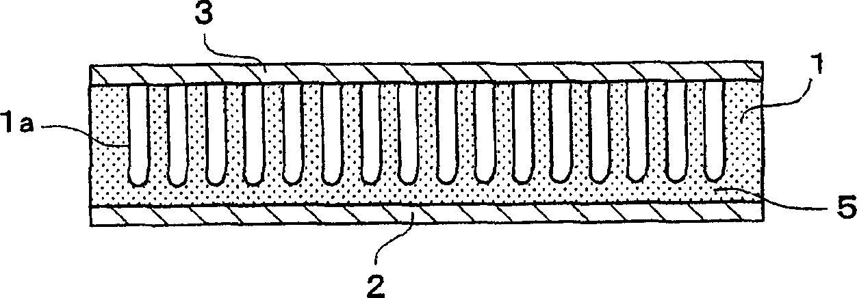
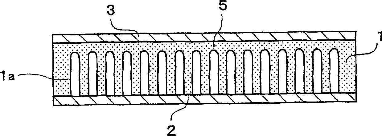
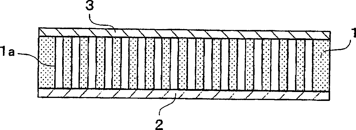
[0067] An Al substrate with a length of 50 mm x a width of 50 mm and a thickness of 2.5 mm was washed with methanol to remove oil, and then immersed in an electrolytic solution of phosphoric acid aqueous solution (phosphoric acid concentration: 4% by weight) kept at 20°C. Then, using the second Al plate as the counter electrode, as shown in Table 1, change the applied voltage (anodization voltage) and time (anodization time) for anodization to form a porous aluminum oxide layer (anodized layer) with nanopores. ). (Sample No.1~23)

[0068] In addition, after anodizing with the applied voltage of 65V, the barrier layer is dissolved by slowly lowering the anodizing voltage, so that the thickness of the barrier layer is less than 10nm, forming an anodic oxidation process in which nanopores penetrate the porous alumina layer substantially. Floor. (Sample No.24~29).

[0069] For the thus formed porous alumina layer having nanopores, the thickness of the nanopore-forming portion a...


PUM


Abstract

An electron source device comprising a porous layer (for example, a porous alumina layer) composed of an insulator and having a plurality of micropores arranged in a direction perpendicular to a main surface; and first and second electrodes arranged on both sides of the porous layer. 2 conductive layers, the current density I / S when the second conductive layer is used as an anode and a DC voltage is applied between the first conductive layer and the first conductive layer is 1 μA / cm2 or more. In the formula, S represents the area of ​​the overlapping portion of the first conductive layer, the second conductive layer, and the porous layer. Since an electron source device with high electron emission capability, low cost, and long life even at a low degree of vacuum can be obtained, a display device with high luminous efficiency and high reliability can be realized.

Description

(1) Technical field [0001] The invention relates to an electron source device and a display device with the electron source device. (2) Background technology [0002] In recent years, as a flat panel type image display device, a field emission display device (hereinafter abbreviated as FED) has been developed. This FED has a front substrate and a rear substrate facing each other with a predetermined gap, three-color fluorescent layers are formed on the inner surface of the front substrate, and an electron emission source for emitting electrons that excite these phosphors is provided on the inner surface of the rear substrate. [0003] So far, a so-called spindt type structure has been proposed as an electron emission source of the FED. This electron emission source has a structure in which an electric field is concentrated at the tip of an electron emission portion formed of molybdenum (Mo), and electrons are emitted from the electron emission portion by a voltage applied b...

Claims


Application Information

Patent Timeline
Patent Type & Authority Applications(China)
IPC IPC(8): H01J29/04H01J1/304H01J1/312H01J9/02H01J31/12
CPCB82Y10/00H01J1/312H01J9/022H01J31/127H01J2201/3125H01J1/304
Inventor 伊藤武夫松田秀三稲村昌晃田中肇坂井和夫
Owner KK TOSHIBA
Why Eureka
Try Eureka