Thermoplastic polyimide resin film, multilayer body and method for manufacturing printed wiring board composed of same

A technology of polyimide resin and resin film, which is applied in printed circuit manufacturing, printed circuit, multilayer circuit manufacturing, etc., and can solve complicated problems

Inactive Publication Date: 2006-01-25
KANEKA CORP
View PDF13 Cites 37 Cited by
  • Summary
  • Abstract
  • Description
  • Claims
  • Application Information

AI Technical Summary

Problems solved by technology

[0012] In this way, when the surface roughness of the film is small, sufficient adhesive strength can be obtained without using expensive or complicated methods, and the adhesive strength can al

Method used


Image

  • Thermoplastic polyimide resin film, multilayer body and method for manufacturing printed wiring board composed of same
  • Thermoplastic polyimide resin film, multilayer body and method for manufacturing printed wiring board composed of same
  • Thermoplastic polyimide resin film, multilayer body and method for manufacturing printed wiring board composed of same

Examples


Embodiment 1~9

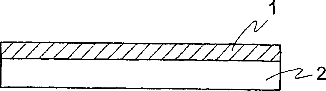
[0277] Coating the polyamic acid solution prepared by manufacturing method X, Y, Z on one side of non-thermoplastic polyimide film A~C with a thickness of 25 μm prepared by polyimide film preparation method A, B, C to make a laminate layers. The thickness of the thermoplastic polyimide layer is 3 μm. The copper foil and the thermoplastic polyimide layer were superimposed, and hot roll lamination was carried out under the conditions of a temperature of 340°C, a line pressure of 20kgf / cm, and a line speed of 1.5m / min. As the copper foil, 18 μm (Rz=1.5 μm) rolled copper foil BHY-22B-T manufactured by Japannagi was used. Next, the laminated copper foil was completely removed with a hydrochloric acid / ferric chloride-based etchant to obtain a laminate in the present invention having a surface-treated thermoplastic polyimide resin film. Determination of surface roughness after surface treatment.

[0278] Next, electroless copper plating and electrolytic copper plating were perform...

Embodiment 10~26

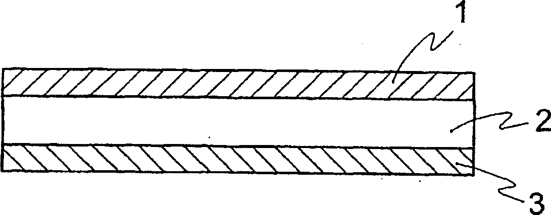
[0284] Experiments were conducted to confirm the effects of various surface treatments. A laminate was prepared by coating one side of a non-thermoplastic polyimide film having a thickness of 25 μm prepared by polyimide film preparation method B with the polyamic acid solution prepared by preparation method Y. The thickness of the thermoplastic polyimide layer is 1, 3, 5 μm.

[0285] (1) Surface treatment with electrodeposited copper foil Electrodeposited copper foil 3EC-VLP foil (thickness 18 μm, Rz=4.6 μm) manufactured by Mitsui Kinzoku Co., Ltd. was laminated in the same manner as in Examples 1 to 9.

[0286] (2) The surface treatment with permanganate was carried out using the permanganate decontamination system manufactured by Artec Co., Ltd. shown in the table below.

[0287]

[0288] process

Treatment liquid composition

processing conditions

swelling

Salinger Krigant (Suering Seki Yurigant) P(*)

...

Embodiment 27-38

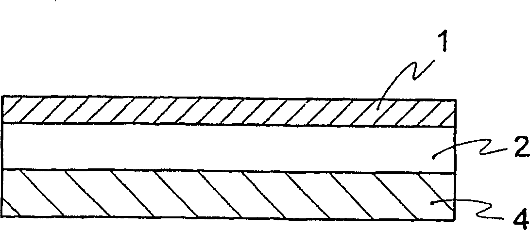
[0300] On both sides of the non-thermoplastic polyimide film C with a thickness of 7.5 μm, 12.5 μm, 25 μm, and 50 μm prepared by the preparation method C of the polyimide film, the polyamic acid solution prepared by the preparation method Y is coated with this method. Laminates formed of thermoplastic polyimide layers of different thicknesses were fabricated. The surface treatment using the copper foil described in Examples 1-9 was performed on this thermoplastic polyimide layer, and the thermal expansion coefficient was measured. Thereafter, electroless plating and electroplating were performed in the same manner as in Examples 1 to 9 to form a copper layer with a thickness of 18 μm, and the adhesive strength at room temperature and the adhesive strength after the pressure cooking test were measured. The results are listed in Table 5. In addition, regarding the thermal expansion coefficient, the thermal expansion coefficient of the non-thermoplastic film C was 12ppm / °C in th...


PUM

PropertyMeasurementUnit
Thicknessaaaaaaaaaa
Thicknessaaaaaaaaaa
Thicknessaaaaaaaaaa

Abstract

The present invention provides a circuit wiring board that has micro wiring circuits and excellent adhesive performance. The board is formed through the following steps: (1) a thermoplastic polyimide layer is formed on one side or both sides of a non-thermoplastic polyimide film so as to form a two-layer or three-layer structure; then Venus treatment is done on the thermoplastic polyimide layer so as to prepare a laminated body; (2) a polymer film is arranged; a layer of the combination of polyimide resin that has a specific structure and polyimide resin that contains thermoset component is arranged on one side or two sides of the film; and (3) at least one side is provided with a resin film and a laminated body thereof; wherein, the resin film has a surface shape, in which Ra1 is 0.05 Mu m to 1 Mu m when the critical value of arithmetic average roughness is 0.002mm and the ratio between Ra1 and Ra2 is 0.4 to 1 when the critical value is 0.1mm.

Description

technical field [0001] The present invention relates to thermoplastic polyimide resin-containing materials, thermoplastic polyimide resin films, laminates, and printed wiring boards containing them, which are widely used in the field of printed wiring boards of electric and electronic equipment, etc. Manufacturing method. Background technique [0002] In recent years, along with higher functions and miniaturization of electronic devices, miniaturization, higher speed, lighter weight, higher density, higher reliability, and the like are also required for electronic components used therein. For this reason, semiconductor element packaging methods and wiring materials or wiring parts for mounting them are also required to be higher density, higher functionality, and higher performance. Therefore, recently, an additive method has been adopted as a method of forming a conductor circuit while multilayering a circuit wiring board. The so-called additive method is a method of form...

Claims


Application Information

Patent Timeline
IPC IPC(8): C08L79/08B32B27/34C23C18/22H05K1/03C08J7/06B32B15/08B32B15/088C08G73/10H05K3/18H05K3/42H05K3/46
Inventor 田中滋伊藤卓西中贤下大迫宽司村上睦明
Owner KANEKA CORP
Why Eureka
Try Eureka