MIS capacitor and production method of MIS capacitor

A capacitor and power supply technology, applied in the field of MIS capacitors, can solve the problems of increasing leakage current, increasing and reducing chip power consumption, and achieving the effect of increasing capacitance and controlling high-frequency noise

A capacitor and power supply technology, applied in the field of MIS capacitors, can solve the problems of increasing leakage current, increasing and reducing chip power consumption, and achieving the effect of increasing capacitance and controlling high-frequency noise

CN1737990AInactive Publication Date: 2006-02-22FUJITSU LTD

Image

  • MIS capacitor and production method of MIS capacitor
  • MIS capacitor and production method of MIS capacitor
  • MIS capacitor and production method of MIS capacitor

Examples


Embodiment Construction

[0025] The preferred embodiments are described in detail below with reference to the drawings.

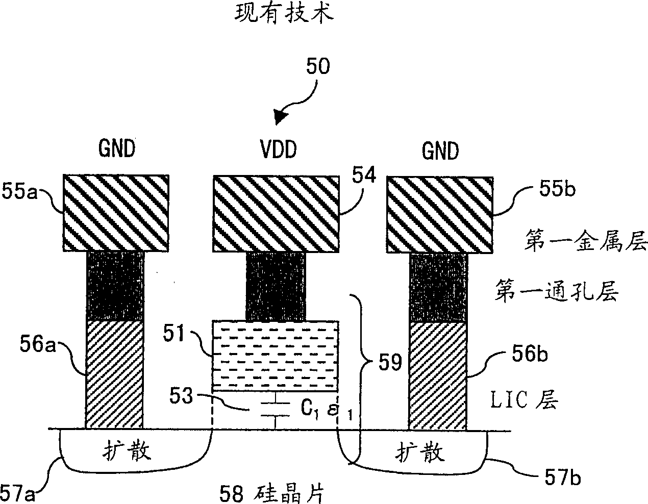
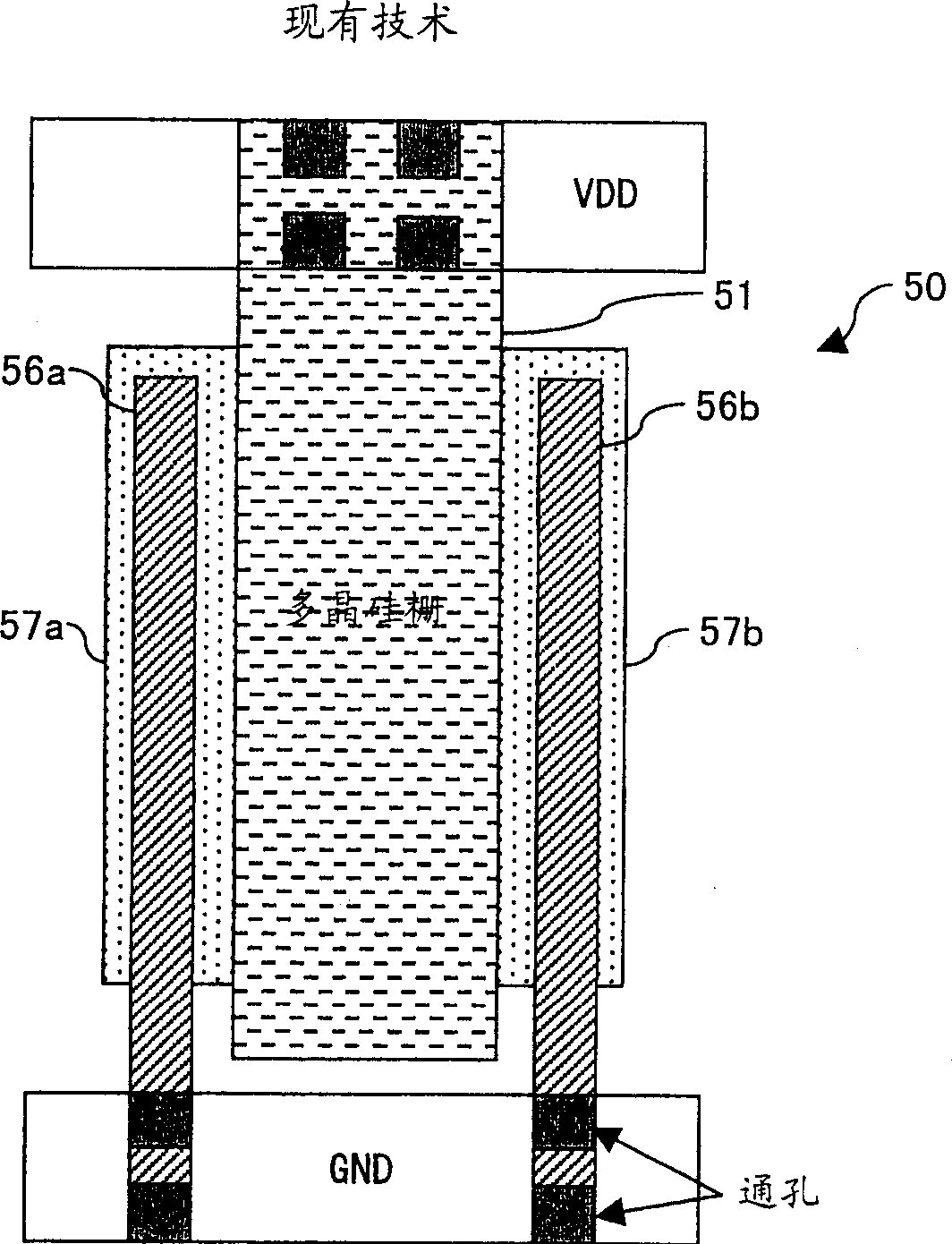
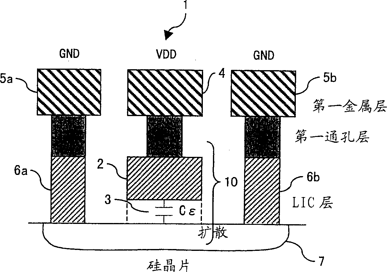
[0026] image 3 It is a cross-sectional view of the MIS (Metal-Insulator-Silicon) capacitor of this embodiment. Figure 4 The top view of the MIS (metal-insulator-silicon) capacitor of this embodiment is shown. On the silicon wafer 8, there are a local interconnection (LIC) layer 2 made of a material such as tungsten, and LIC layers 6 a and 6 b directly bonded on the silicon wafer 8. The LIC layer 2 is bonded on the silicon wafer 8 through an oxide film such as a field oxide film 3. The wiring layer 4 connected to the power supply wiring VDD is provided on the first via layer mounted on the LIC layer 2. The wiring layers 5a and 5b connected to the power wiring GND are respectively provided on the first via layer mounted on the LIC layers 6a and 6b. A diffusion region 7 is formed on the surface of the silicon wafer 8 connected to the field oxide film 3 between the LIC layer 2 and the s...


PUM


Abstract

The present invention provides a MIS capacitor and a production method of MIS capacitor. A silicon wafer, with a diffusion area formed in a predetermined region on one side, comprises a lower electrode of a capacitor unit. A first metal layer is connected to a first power supply wiring (VDD) and comprises an upper electrode of the capacitor unit. Second metal layers are connected to a second power supply wiring (GND) and are also formed on the side where diffusion area is formed on silicon wafer. An oxide film is placed between the first metal layer and the surface of the silicon wafer where the diffusion area is formed.

Description

Technical field [0001] The present invention relates to a MIS (metal-insulator-silicon) capacitor and a manufacturing method of the MIS capacitor. Background technique [0002] It is mentioned in Japanese Patent Laid-Open No. 6-21263 that a plurality of logic cells mounted on an integrated circuit are connected to the power supply wiring VDD and the power supply wiring GND and mounted on the integrated circuit. The area between the logic cells is the formation area of ​​the metal wiring for connection based on the logical connection information. [0003] The crosstalk noise between wirings and the simultaneous switch noise of the transistors (simultaneous switch noise) often cause voltage changes in the power wiring voltage on the integrated circuit. This voltage change causes a decrease in the operating speed of the transistor and malfunctions. In view of this, in order to control the voltage change, Japanese Patent Laid-Open No. 2001-185624 discloses a technique of installing a...

Claims


Application Information

Patent Timeline
22 Feb 2006
Publication
CN1737990A
IPC
H01L21/00; H01L21/02; H01L29/00; H10B12/00
CPC
H01L27/0811; H01L29/94; H01L29/417; H01L27/04; H01L21/00
Inventors
ε˜‰ε–œζ‘ι–; 村谷惠介