Chemical mechanical polishing technique

A grinding process and chemical-mechanical technology, used in grinding devices, grinding machine tools, other chemical processes, etc., can solve problems such as low dielectric scratches, structural cracks, increased maintenance costs, and increased parts costs

Inactive Publication Date: 2006-04-05
UNITED MICROELECTRONICS CORP
View PDF1 Cites 13 Cited by
  • Summary
  • Abstract
  • Description
  • Claims
  • Application Information

AI Technical Summary

Problems solved by technology

[0007] Furthermore, in order to increase the output rate, the prior art disclosed in the above-mentioned US patent uses a relatively high downward force in the first step, which may cause scratches on the fragile low dielectric constant layer below, and even cause structural dam

Method used


Image

  • Chemical mechanical polishing technique
  • Chemical mechanical polishing technique
  • Chemical mechanical polishing technique

Examples


Embodiment Construction

[0028] The invention relates to a method for forming high-reliability integrated circuit metal interconnection, especially aimed at improving the chemical mechanical polishing process applied to copper / barrier layer embedded metal interconnection in the back-end process of integrated circuit. It should be noted that “copper” referred to below generally refers to copper metal or any copper alloy material suitable for the copper damascene process. The main advantages of the present invention are high throughput, especially at the CMP stage, and low cost.

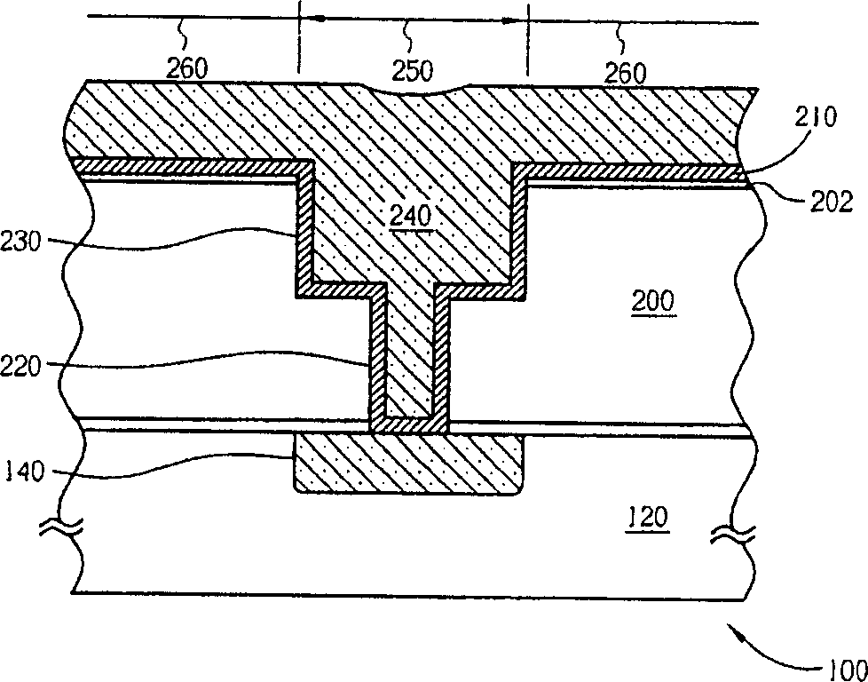
[0029] For clarification, see figure 2 , which shows a schematic cross-sectional view of the semiconductor wafer 100 before performing the CMP process of the present invention, on which the copper metal layer 240 and the barrier layer 210 are formed. Such as figure 2 As shown, the barrier layer 210 is formed on the surface of the damascene recessed region 250 and formed on the uppermost surface region 260 of the dielectric...


PUM


Abstract

The invention provides a chemical mechanical milling process comprising following steps: first, loading the wafers which has lines of metal layer and baffle layer; then, via one first milling cushion, milling the metal layer in same milling speed to expose the lower baffle layer, wherein, the first milling paste distributed on the first milling layer has high milling selective rate to the baffle layer; the second milling step that utilizing one second milling cushion and the second milling past to mill and remove the exposed baffle layer. According to said invention, the milling selective rate (the copper to baffle layer) of first milling past is at least more than 30 while the better is more than 100.

Description

technical field [0001] The invention relates to the field of semiconductor manufacturing technology, in particular to a chemical mechanical polishing process for copper / barrier layer metal interconnection lines. Background technique [0002] In recent years, due to the maturity of the copper damascene process technology, the integrated circuit manufacturing can continue to flourish after entering the deep submicron and nanometer generations, and reach a mass production scale with high yield. As known by those skilled in the art, the copper damascene interconnection process basically includes deposition of a dielectric layer, photolithography and etching to define a wire trench structure, barrier layer coating, formation of a copper seed layer, and copper metal electroplating. Finally, the excess copper metal deposited outside the wire trench structure is removed by chemical mechanical polishing (CMP) technology. [0003] When carrying out the aforementioned CMP process, usu...

Claims


Application Information

Patent Timeline
IPC IPC(8): H01L21/304B24B1/00B24B37/00C09K3/14B24B37/10
Inventor 许嘉麟蔡胜群
Owner UNITED MICROELECTRONICS CORP
Why Eureka
Try Eureka