

Semiconductor laser
A technology of lasers and semiconductors, applied in the direction of semiconductor lasers, lasers, laser components, etc., can solve the problems of high threshold current and unsatisfactory problems, and achieve the effect of suppressing backhaul optical noise
- Summary
- Abstract
- Description
- Claims
- Application Information
AI Technical Summary
Problems solved by technology
Method used
Image

Examples
Embodiment 1
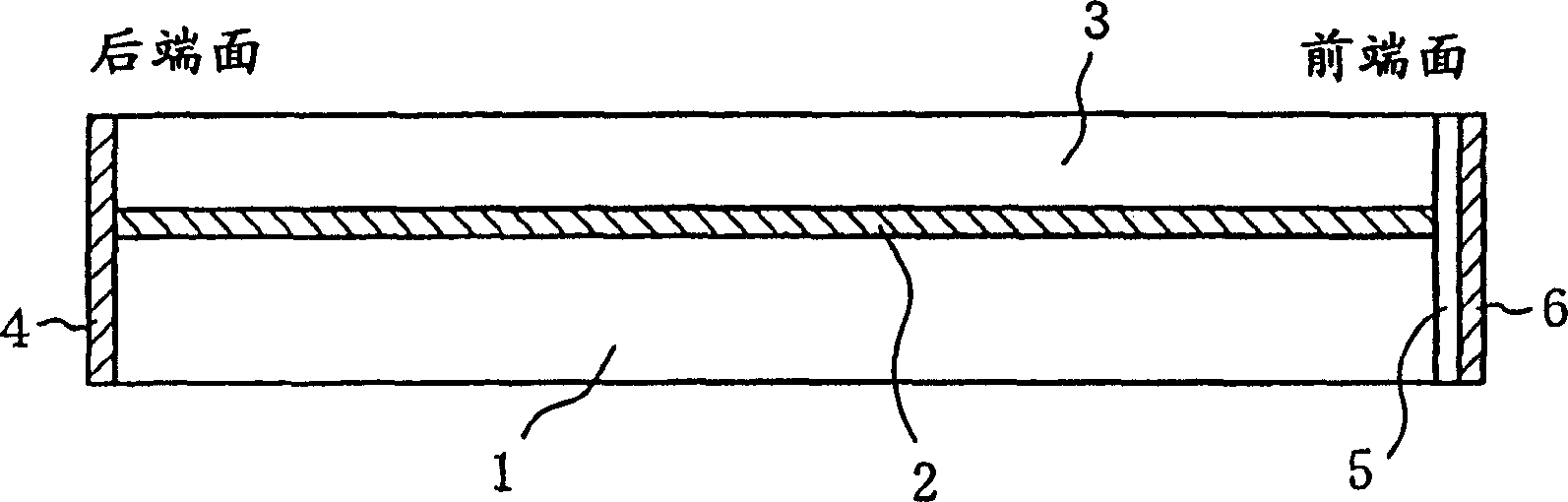
[0023] figure 1 It is a cross-sectional view showing a schematic structure of the semiconductor laser according to Embodiment 1 of the present invention.
[0024] In the figure, 1 represents a p-type InP substrate, 2 represents an active layer composed of InGaAsP, and 3 represents a cladding layer composed of n-type InP. Here, one layer is used to represent the active layer 2, but the active layer 2 may be multiple quantum wells. In addition, beam binding layers for adjusting the boundary distribution of light may be provided above and below the active layer 2 . In this example, the conductivity type of the substrate 1 is p-type, but the polarity can also be reversed, and a structure in which an active layer and a p-type InP cladding layer are arranged on an n-type InP substrate can be adopted. SiO 2 , Si, Al 2 o 3 A multilayer high reflection film 4 having a reflectance of about 90% is formed, and a laminated film composed of a first dielectric film 5 and a second diele...
Embodiment 2
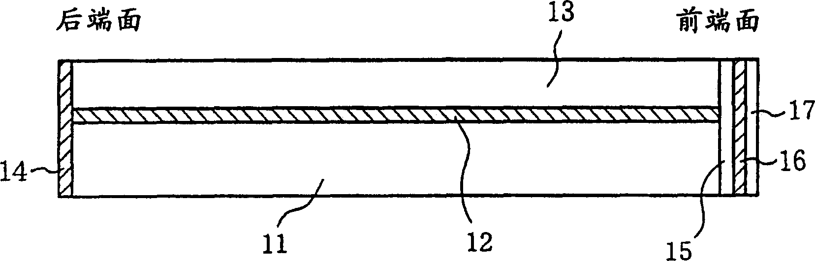
[0038] image 3 It is a cross-sectional view showing a schematic structure of a semiconductor laser according to Embodiment 2 of the present invention.
[0039] In the figure, 11 denotes a p-type InP substrate, 12 denotes an active layer made of InGaAsP, and 13 denotes a cladding layer made of n-type InP. The structure of the reflective film 14 formed on the rear end face is the same multilayer high reflective film as in the first embodiment described above. A laminated film of various dielectric materials consisting of a first dielectric film 15 , a second dielectric film 16 , and a third dielectric film 17 is formed on the front end surface to be the laser light emitting surface. As an example of the structure of this laminated film, the first dielectric film 15 is made of SiO with a thickness of λ / 4 (λ represents the wavelength in the medium of the LD oscillation light). 2 film, the second dielectric film 16 adopts Al with a thickness of λ / 4 2 o 3 film, the third dielec...
Embodiment 3
[0045] Figure 5 It is a cross-sectional view showing a schematic structure of a semiconductor laser according to Embodiment 3 of the present invention.
[0046] In the figure, 21 represents a p-type InP substrate, 22 represents an active layer composed of InGaAsP, 23 represents a cladding layer composed of n-type InP, and 24 represents a diffraction grating composed of n-type InGaAsP disposed in the laser resonator. The structure of the rear end face reflective film 25 is the same multi-layer high reflective film as in the first embodiment described above. A first dielectric film 26 and a second dielectric film 27 are formed on the front end surface. The material and thickness of the dielectric film are the same as in Example 1 above.
[0047] As described above, according to the third embodiment, a multilayer film composed of various dielectric materials described in the first or second embodiment is formed on the laser emission surface of the DFB-LD having a diffraction g...
PUM
 Abstract
Description
Claims
Application Information