

Multilayer printed wiring board
A multi-layer printing and circuit board technology, applied in the direction of multi-layer circuit manufacturing, circuits, electrical components, etc., can solve the problems of narrowed insulation interval, poor insulation reliability, etc., to reduce loop inductance, high insulation reliability, and miniaturization. and the effect of preventing power shortage
- Summary
- Abstract
- Description
- Claims
- Application Information
AI Technical Summary
Problems solved by technology
Method used
Image

Examples
no. 1 Embodiment
[0095] [First Example] Glass epoxy substrate
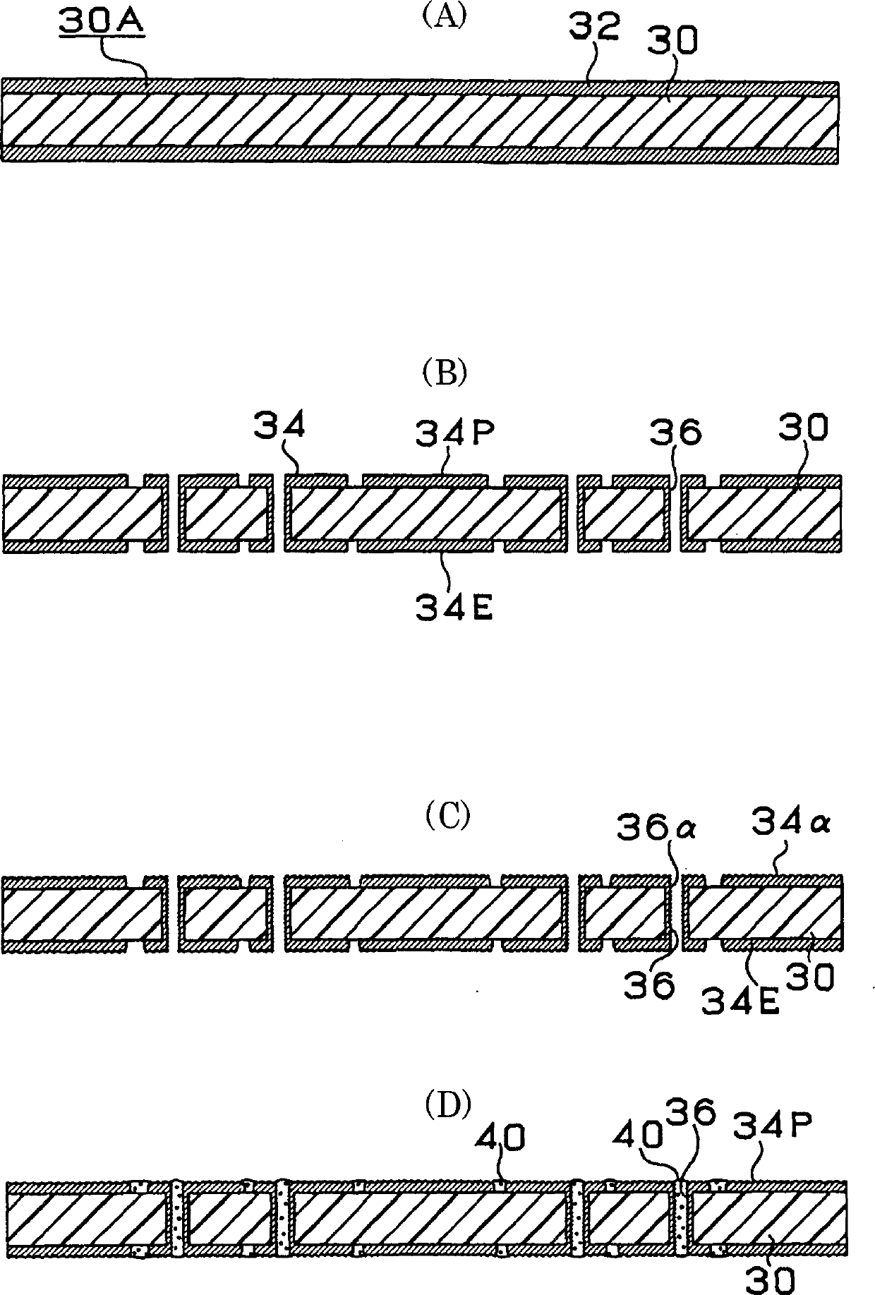
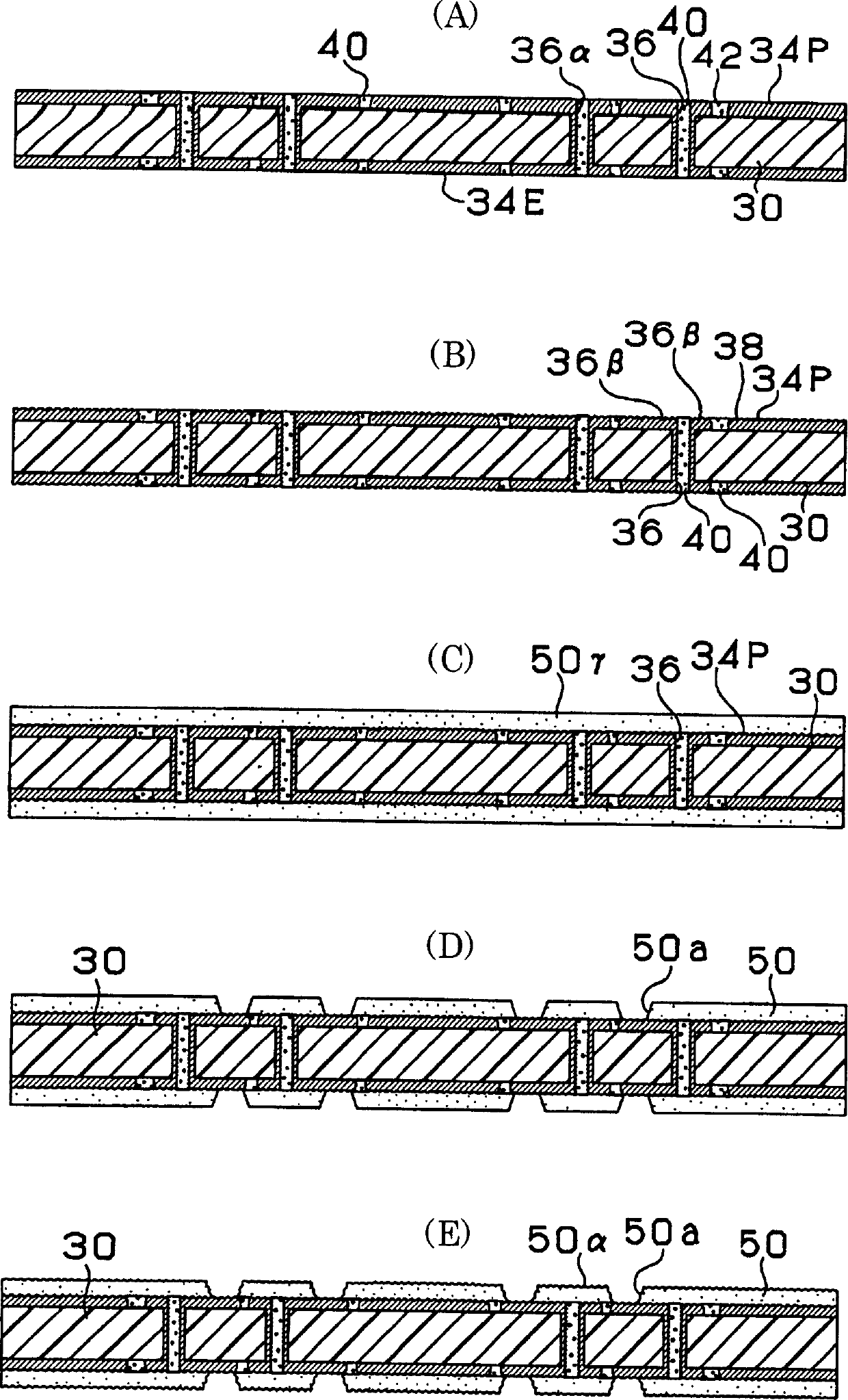
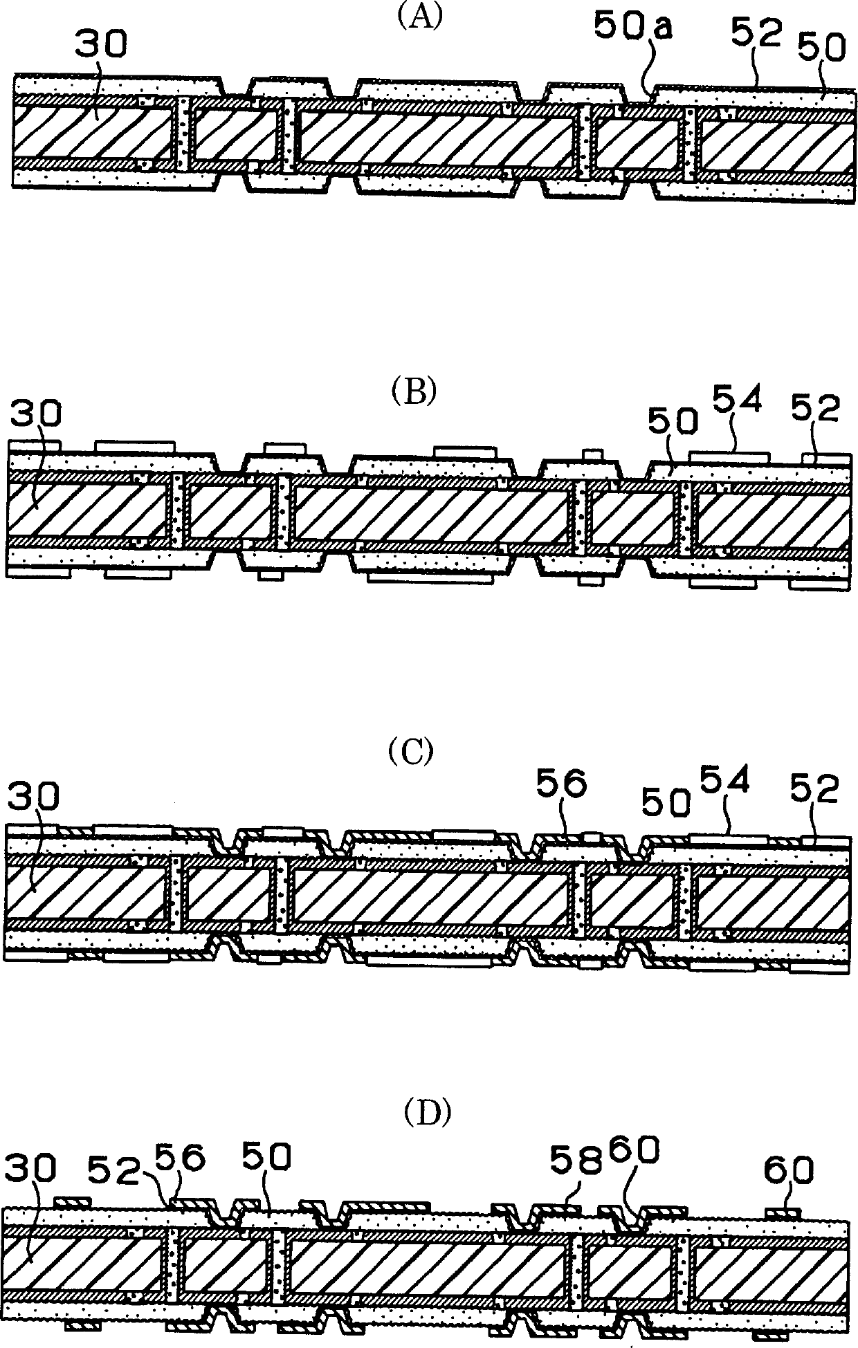
[0096]First, the structure of a multilayer printed circuit board 10 according to a first embodiment of the present invention will be described with reference to FIGS. 1 to 7 . 6 is a cross-sectional view showing the multilayer printed circuit board 10 , and FIG. 7 shows a state in which the IC chip 90 is mounted on the multilayer printed circuit board 10 shown in FIG. 6 and placed on a daughter board 94 . As shown in FIG. 6 , in multilayer printed wiring board 10 , conductive circuit 34 and conductive layer 34P are formed on the front surface of core substrate 30 , and conductive circuit 34 and conductive layer 34E are formed on the back surface thereof. The upper conductor layer 34P is formed as a power supply plane layer, and the lower conductor layer 34E is formed as a ground plane layer. The front and back surfaces of the core substrate 30 are connected by via holes 36 . In addition, the interlayer resin insulating layer 50 ...
no. 1 Embodiment -1
[0104] A. Manufacture of resin film for interlayer resin insulating layer
[0105] Bisphenol A type epoxy resin (455 epoxy equivalents, Epikote 1001 manufactured by (油化シェルエポキシ company)) 29 parts by weight, cresol-novolak type epoxy resin (215 epoxy equivalents, Dainippon Ink Chemical Industry Co., Ltd. 39 parts by weight of Epikuron (Epikuron) N-673), 30 parts by weight of phenol novolac resin (phenolic hydrocarbon group equivalent 120, Dainippon Ink Chemical Industry Co., Ltd. phenate KA-7052) containing a triazine structure, heated and melted while stirring To 20 parts by weight of diethylene glycol ethyl ether acetate and 20 parts by weight of solvent naphtha, 15 parts by weight of terminally epoxidized polybutadiene rubber (Tenarekkusu R-45EPT manufactured by Nagase Chemical Industry Co., Ltd.) and 2 parts by weight were added. - 1.5 parts by weight of pulverized phenyl-4,5-bis(hydroxymethyl)imidazole, 2.5 parts by weight of finely ground silica, and 0.5 parts by weight of...
no. 1 Embodiment -2
[0156] Although it is the same as the first embodiment-1 described with reference to FIG. 6 , it is manufactured as follows.
[0157] Thickness of conductor layer of core substrate: 55 μm
[0158] Thickness of the power supply layer of the core substrate: 55 μm
[0159] Thickness of the conductor layer of the interlayer insulating layer: 15 μm
PUM
 Abstract
Description
Claims
Application Information