Thin film transistor and method for manufacturing the same

A technology of thin-film transistors and manufacturing methods, which is applied in the direction of transistors, semiconductor/solid-state device manufacturing, photolithography process exposure devices, etc., and can solve the problems of cumbersome and time-consuming manufacturing process steps

Inactive Publication Date: 2006-06-21
CHUNGHWA PICTURE TUBES LTD
View PDF0 Cites 18 Cited by
  • Summary
  • Abstract
  • Description
  • Claims
  • Application Information

AI Technical Summary

Problems solved by technology

[0005] In view of this, the object of the present invention is to provide a method for manufacturing a thin film transistor to solve the problem of complicated and time-consuming manufacturing process steps in the known

Method used


Image

  • Thin film transistor and method for manufacturing the same
  • Thin film transistor and method for manufacturing the same
  • Thin film transistor and method for manufacturing the same

Examples


no. 1 example

[0015] Figure 2A to Figure 2C It is a schematic cross-sectional view of a manufacturing process of a thin film transistor according to a preferred embodiment of the present invention.

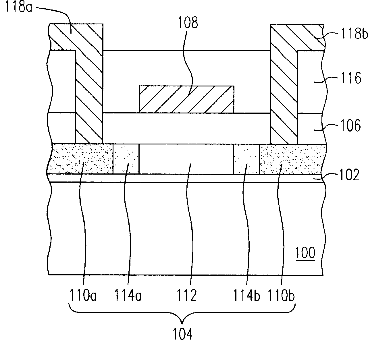
[0016] First, please refer to Figure 2A , sequentially forming a polysilicon layer 204 and a gate dielectric layer 206 on the substrate 200 . Wherein, the substrate 200 is, for example, a transparent substrate, such as glass. In addition, the polysilicon layer 204 is formed by, for example, first forming an amorphous silicon layer (not shown in the figure) on the substrate 200, and then performing an Excimer Laser Annealing (ELA) process, so that the amorphous silicon layer The polysilicon layer 204 is formed by melting and recrystallization. In addition, the material of the gate dielectric layer 206 is, for example, silicon nitride, silicon oxide, silicon oxynitride or other suitable materials, and its formation method is, for example, a chemical vapor deposition process. In addition, in...

no. 2 example

[0026] In the following description, the parts with the same marks as those of the above-mentioned embodiments will not be repeated.

[0027] Figure 6A to Figure 6D It is a schematic cross-sectional view of the manufacturing process of another thin film transistor according to a preferred embodiment of the present invention.

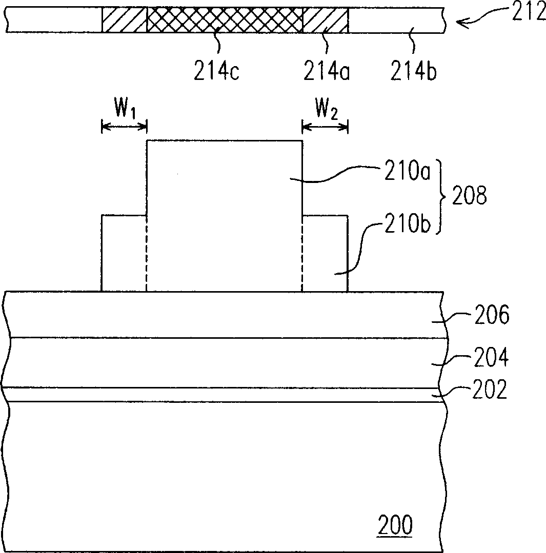
[0028] First, please refer to Figure 6A , sequentially forming a polysilicon layer 204 , a gate dielectric layer 206 and a gate layer 226 on the substrate 200 . In a preferred embodiment, before forming the polysilicon layer 204 , it further includes forming a buffer layer 202 on the substrate 200 .

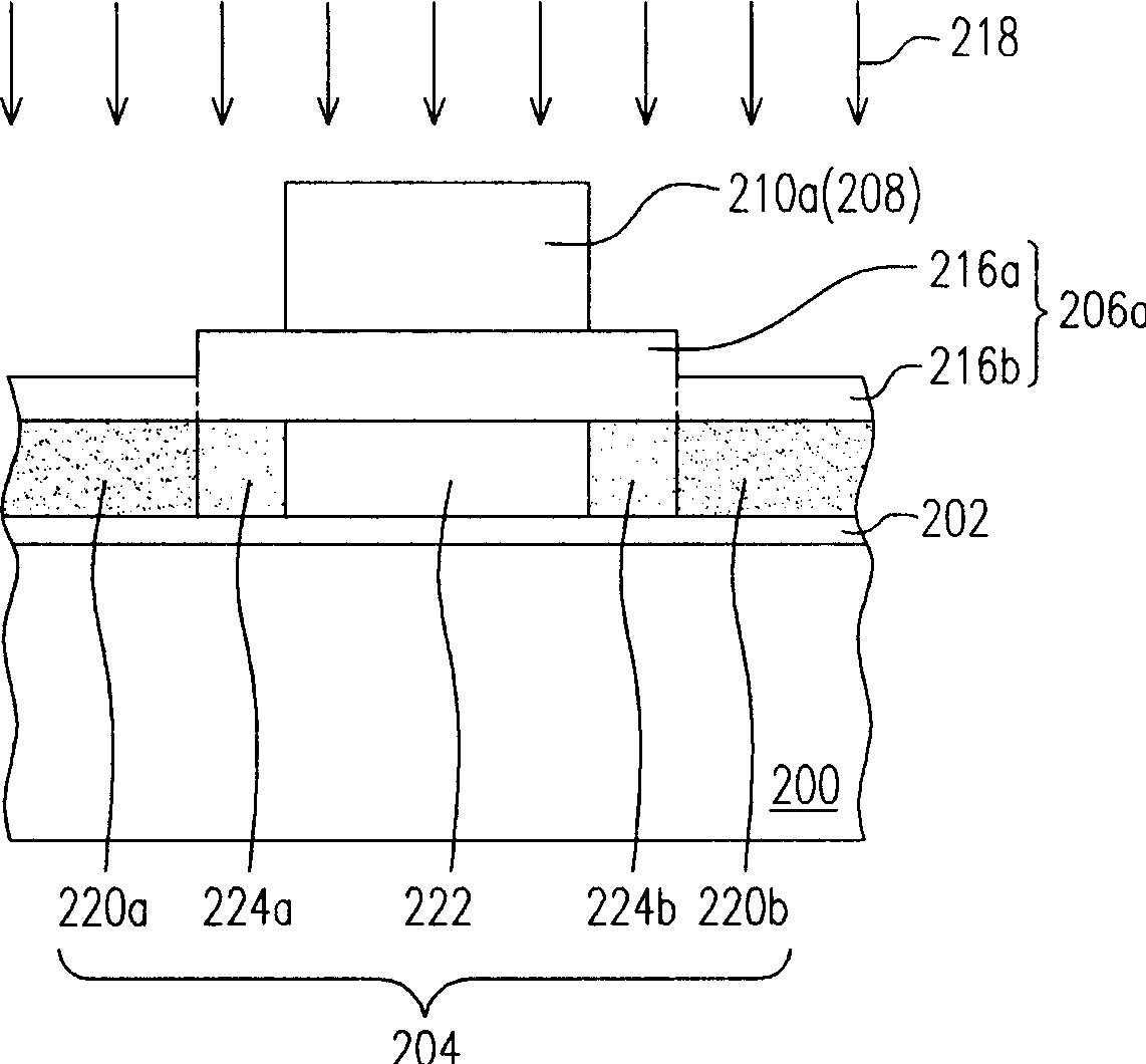
[0029] Next, a patterned photoresist layer 208 is formed on the gate layer 226 . Wherein, the patterned photoresist layer 208 has a first portion 210a and a second portion 210b, and the second portion 210b is located on both sides of the first portion 210a, and its thickness is smaller than that of the first portion 210a . In addition, the formation ...

no. 3 example

[0044] In the following description, the parts with the same marks as those of the above-mentioned embodiments will not be repeated.

[0045] Figure 13A to Figure 13D It is a schematic cross-sectional view of another manufacturing process of a thin film transistor according to a preferred embodiment of the present invention.

[0046] First, please refer to Figure 13A , sequentially forming a polysilicon layer 204 , a gate dielectric layer 206 and a gate layer 226 on the substrate 200 . In a preferred embodiment, before forming the polysilicon layer 204 , it further includes forming a buffer layer 202 on the substrate 200 .

[0047] Next, a patterned photoresist layer 208 is formed on the gate layer 226 . Wherein, the patterned photoresist layer 208 has a first portion 210a and a second portion 210b, and the second portion 210b is located on both sides of the first portion 210a, and its thickness is smaller than that of the first portion 210a . In addition, the formation...


PUM


Abstract

The invention discloses a film crystal pipe, which comprises the following parts: base, polysilicon layer, patterning grate dielectric layer, grid layer, source polar region, drain region and light dope drain region, wherein the polysilicon layer is set on the base; the patterning grate dielectric layer is set on the polysilicon layer, which possesses the third and fourth parts with the thickness of the third part less than the thickness of the fourth part; the grid layer is set on part of the patterning grate dielectric layer; the source polar region and drain region are set in the polysilicon layer corresponding to the fourth part of patterning grate dielectric layer; the corresponding part of grid layer and polysilicon layer is channel region; the light dope drain region is set in the polysilicon layer corresponding to the third part of patterning grate dielectric layer.

Description

technical field [0001] The present invention relates to a semiconductor element and its manufacturing method, and in particular to a thin film transistor and its manufacturing method. Background technique [0002] In common components, a switch is required to drive the operation of the component. Taking the active display element as an example, it usually uses a thin film transistor (Thin Film Transistor, TFT) as a driving switch. The thin film transistors can be further divided into amorphous silicon (Amorphous Silicon, a-Si) thin film transistors and polysilicon (Poly-Silicon) thin film transistors according to the material of the channel region. Among them, polysilicon thin film transistors have lower power consumption and higher electron mobility than amorphous silicon thin film transistors. Moreover, due to the recent development of laser technology, the manufacturing process temperature of polysilicon thin film transistors has dropped below 600 degrees Celsius, so po...

Claims


Application Information

Patent Timeline
Patent Type & Authority Applications(China)
IPC IPC(8): G03F7/20H01L21/00H01L29/786
Inventor 张锡明沈嘉男
Owner CHUNGHWA PICTURE TUBES LTD
Why Eureka
Try Eureka