Supercharge Your Innovation With Domain-Expert AI Agents!

Components for substrate processing apparatus and manufacturing method thereof

A substrate processing device and manufacturing method technology, which is applied in semiconductor/solid-state device manufacturing, electrical components, plasma, etc., can solve the problems of focusing ring consumption and deformation, and achieve the effect of preventing the decline of operation rate and reducing the particle generation rate

Inactive Publication Date: 2006-06-21
TOKYO ELECTRON LTD
View PDF1 Cites 6 Cited by
  • Summary
  • Abstract
  • Description
  • Claims
  • Application Information

AI Technical Summary

Problems solved by technology

[0004] However, as the silicon is eroded by the plasma, in the chamber, the focus ring consumes deformation in a short time

Method used


Image

  • Components for substrate processing apparatus and manufacturing method thereof
  • Components for substrate processing apparatus and manufacturing method thereof
  • Components for substrate processing apparatus and manufacturing method thereof

Examples


Embodiment Construction

[0065] Hereinafter, embodiments of the present invention will be described with reference to the drawings.

[0066] First, a component for a substrate processing apparatus and a manufacturing method thereof according to a first embodiment of the present invention will be described.

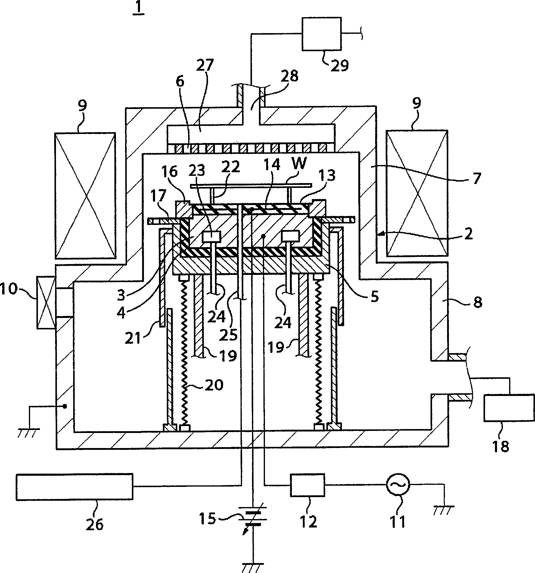
[0067] figure 1 It is a cross-sectional view showing a schematic structure of a substrate processing apparatus using a focus ring as a substrate processing apparatus component according to the first embodiment of the present invention.

[0068] figure 1 Among them, the etching processing apparatus 1 constituted as a substrate processing apparatus has: for example, an aluminum cylindrical chamber 2; The support body 5 of the lower electrode 3 that can be lifted freely; and the shower head 6 that is arranged above the chamber 2 as the upper electrode opposite to the lower electrode 3 .

[0069] The upper part of the chamber 2 is formed as an upper chamber 7 with a smaller diameter, and the lower ...


PUM


Abstract

The present invention provides a method of manufacturing a component for a substrate processing apparatus that can suppress the generation of particles, prevent a decrease in the operating rate of the substrate processing apparatus, and can be easily manufactured. A focus ring is formed by cutting silicon carbide formed by a sintering method or a CVD method (step S31), and the formed focus ring is exposed to at least one of carbon tetrafluoride gas and oxygen as impurities. In the plasma generated by this kind of gas, the impurity is introduced into the hole-shaped defects existing near the surface of the focus ring (step S32), and the positron is injected into the vicinity of the surface of the focus ring into which the impurity is introduced, and the positron The defect existence ratio near the surface of the focus ring is checked by the electron annihilation method (step S33).

Description

technical field [0001] The present invention relates to a component for a substrate processing apparatus and a manufacturing method thereof, and particularly to a substrate processing apparatus component used in a consumable environment and a manufacturing method thereof. Background technique [0002] Generally, a substrate processing apparatus for performing an etching process on a semiconductor wafer (hereinafter referred to as "wafer") as a substrate has a storage chamber (hereinafter referred to as "chamber") for storing the wafer. In this substrate processing apparatus, high-frequency power is applied to the chamber, and CF 4 A process gas such as a gas-like gas is used to generate plasma, and the wafer surface is etched using the generated plasma. [0003] Various components for maintaining the state of the plasma in a desired state are arranged in the chamber, and a focus ring is known as one of such components. The focus ring is an annular member, and is disposed i...

Claims


Application Information

Patent Timeline
IPC IPC(8): H01L21/00C23F4/00H01L21/02H01L21/3065
CPCH01J37/32642C04B41/0054C04B41/009C04B41/80C04B35/565
Inventor 守屋刚三桥康至上殿明良
Owner TOKYO ELECTRON LTD
Features
  • R&D
  • Intellectual Property
  • Life Sciences
  • Materials
  • Tech Scout
  • Unparalleled Data Quality
  • Higher Quality Content
  • 60% Fewer Hallucinations
Learn More