Nondestrutive detection method of microregion residual stress

A residual stress, non-destructive testing technology, applied in special data processing applications, material analysis using radiation diffraction, instruments, etc., can solve the problem of long time, reduce measurement time, reduce time consumption, and facilitate the promotion and application.

Inactive Publication Date: 2006-06-28
HARBIN INST OF TECH
View PDF0 Cites 36 Cited by
  • Summary
  • Abstract
  • Description
  • Claims
  • Application Information

AI Technical Summary

Problems solved by technology

[0006] In view of the shortcomings of the traditional XRD residual stress detection method, which is time-consuming and needs to use high-angle diffraction peaks to ensure the diffraction intensity, and now using XRD 2 There are problems with the same shortcomings as above in equipment measurement. The present invention provides a non-destructive testing method for residual stress in small areas of crystalline bulk and thin film materials with fast measurement speed and high precision.

Method used


Image

  • Nondestrutive detection method of microregion residual stress
  • Nondestrutive detection method of microregion residual stress
  • Nondestrutive detection method of microregion residual stress

Examples


specific Embodiment approach 1

[0010] Specific implementation mode 1: In this implementation mode, an XRD equipped with a small X-ray point source and a two-dimensional plane X-ray detector is utilized. 2 Equipment, adjust the X-ray spot diameter (30 μm ~ 10mm) and the measurement area, according to the equipment to determine the X-ray tube voltage and tube current are 30 ~ 60kV and 35 ~ 45mA. The purpose is to realize the fast residual stress detection in the tiny area.

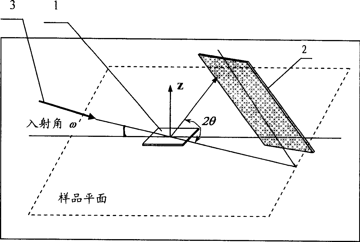
[0011] This embodiment is directed to crystalline bulk materials. First, adjust the XRD 2 The optical path and collimation system of the equipment meet the hardware requirements for determining residual stress. The second step is to install the sample required to determine the residual stress on the equipment sample test bench. The sample 1 is placed horizontally, and the XRD 2 The X-ray plane detector 2 on the equipment is arranged at an acute angle with the horizontal plane towards the direction of the sample to be measured, and the ...

specific Embodiment approach 2

[0012] Specific embodiment two: the difference between this embodiment and specific embodiment one is that the Pb(Zr 52 Ti 48 )O 3 The film was tested, and the film crystallized into a perovskite phase at 650°C. During the measurement, the incident angle ω was selected as 18°, the X-ray spot diameter was adjusted to 100 μm, the X-ray tube voltage and tube current were 40 kV and 40 mA, respectively, and the scanning time was 1 minute.

specific Embodiment approach 3

[0013] Embodiment 3: The difference between this embodiment and Embodiment 1 and Embodiment 2 is that the detection is performed on crystalline ZnO or TiN or Au thin film materials, and the measurement method is the same as Embodiment 1.

[0014] Principle of the present invention is as follows:

[0015] The XRD adopted in the non-destructive testing method of residual stress in the present invention 2 The schematic diagram of the optical path of the device is shown in figure 1 As shown, the two-dimensional planar X-ray detector forms an acute angle with the horizontal direction to receive the scattered signal from the sample. The test sample is placed horizontally, the X-ray incident angle is ω, and the spot position and diameter of the X-ray can be adjusted (30μm~ 10mm), to measure the residual stress of different tiny areas on the surface of the sample.

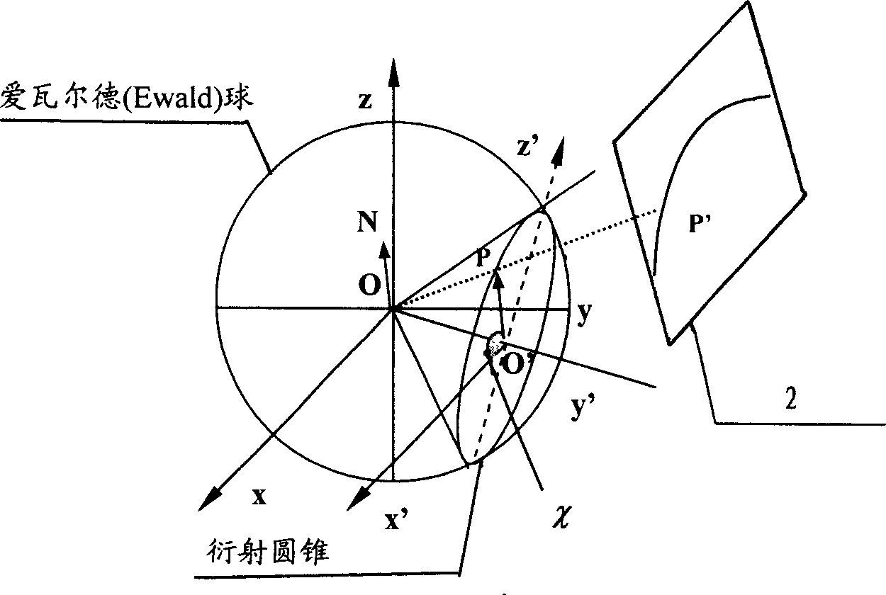
[0016] figure 2 for XRD 2 Schematic diagram of the principle of two-dimensional surface detection diffraction. For...


PUM

PropertyMeasurementUnit
diameteraaaaaaaaaa
diameteraaaaaaaaaa
residual stressaaaaaaaaaa

Abstract

A method for nondestructively detecting residual stress on micro region includes utilizing XRD2 device to measure sample with residual stress to be tested to obtain XRD2 surface exploring atlas, then processing obtained atlas for obtaining a set of diffraction angle data varied in flowing Debye field angle variation at diffraction peak, obtaining relevant straight by using linear function to adapt data and obtaining relation of straight line slope to residual stress by adapting so as to calculate out residual stress of micro-region on measured sample.

Description

technical field [0001] The present invention relates to a non-destructive detection method for micro-area stress, in particular to a method for non-destructive measurement of residual stress in micro-area of ​​crystalline bulk and film materials by using an X-ray diffraction device equipped with a small point light source and a two-dimensional plane X-ray detector method. Background technique [0002] Macroscopic residual stress widely exists in materials, devices and parts, and is an important factor affecting the performance of parts, and even leads to failure accidents. In recent years, thin film materials have been widely used in the fields of information, electromechanical, aerospace and aviation due to their special effects such as acousto-optic, electromagnetic and mechanical. However, device fatigue and performance degradation related to residual stress have always restricted the practical application of functional thin films. The bottleneck has become a difficult p...

Claims


Application Information

Patent Timeline
Patent Type & Authority Applications(China)
IPC IPC(8): G01N23/20G06F19/00
Inventor 费维栋杨帆
Owner HARBIN INST OF TECH
Why Eureka
Try Eureka