
Dimesize dynamic piezoresistance, pressure sensor, and manufacturing method
A pressure sensor, dynamic piezoresistive technology, applied in chemical instruments and methods, fluid pressure measurement by changing ohmic resistance, measurement of fluid pressure, etc., to achieve excellent anti-light interference, protection against destructive impact, and improved performance.
- Summary
- Abstract
- Description
- Claims
- Application Information
AI Technical Summary
Problems solved by technology
Method used
Image


Examples
Embodiment Construction
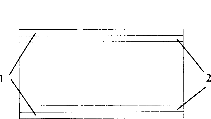
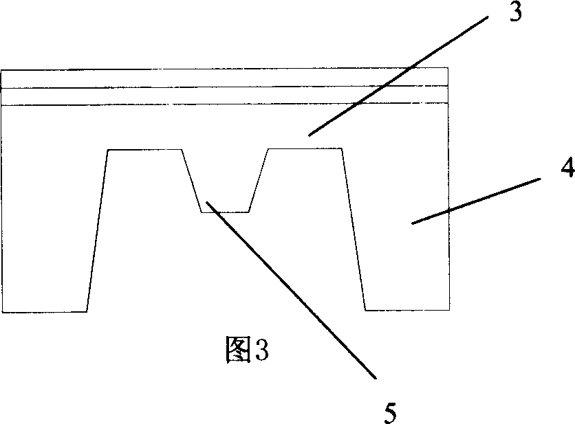
[0054] Using MEMS silicon micromachining technology to manufacture miniature pressure sensitive chips, the unit size of the chip is 1.5×1.5, the size of the sensitive diaphragm is 1.0×1.0, and an island-shaped hard core is left in the center of the diaphragm, and the size of the hard core is 0.7 ×0.7, the force-sensitive detection resistor is distributed on the film between the hard core and the boundary hard frame, and the position is determined according to the design method of the E-type sensitive chip. The implementation steps are as follows Figure 1 to Figure 5 The implementation shown:
[0055] figure 1 The double-sided polished silicon wafer used as an elastic element is covered with 1 μm thick SiO on both sides by traditional thermal oxidation technology in MEMS technology processing. 2 Layer 2, and then use standard LPCVD method to cover 3000A thick Si on both sides 3 N 4 Layer 1, use two photolithography techniques to etch away the Si on the back of the silicon ...
PUM
| Property | Measurement | Unit |
|---|---|---|
| thickness | aaaaa | aaaaa |
| thickness | aaaaa | aaaaa |
Abstract
Description
Claims
Application Information