

Solid-state imaging device and its manufacturing method
A technology of a solid-state imaging device and a manufacturing method, which is applied in semiconductor/solid-state device manufacturing, electrical components, image communication, etc., and can solve problems such as defects and difficulty in miniaturizing the imaging area 107
- Summary
- Abstract
- Description
- Claims
- Application Information
AI Technical Summary
Problems solved by technology
Method used
Image

Examples
no. 1 Embodiment approach
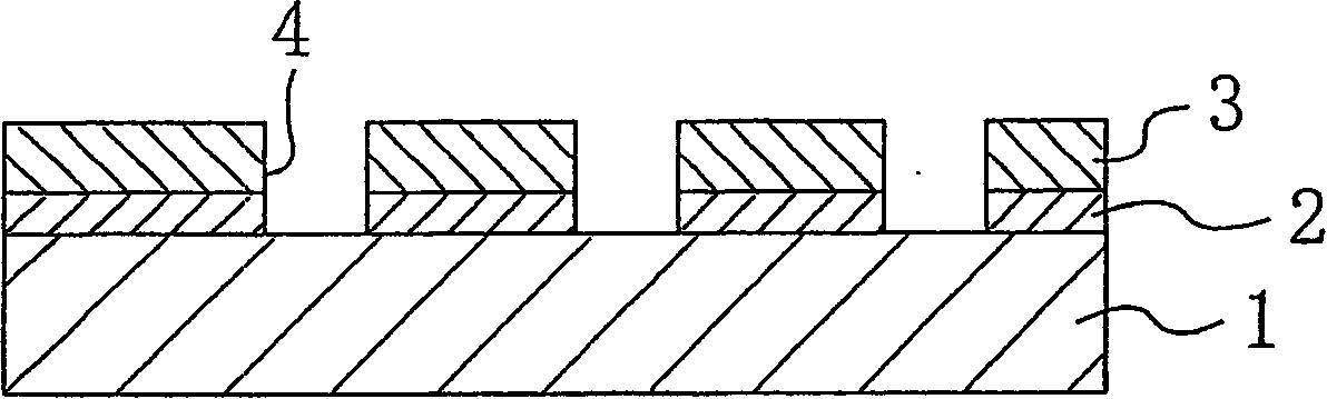
[0118] Figure 1A ~ Figure 1F It is a cross-sectional view showing a step of forming an element isolation region in the manufacturing process of the solid-state imaging device according to the first embodiment.
[0119] In the manufacturing process of the solid-state imaging device of this embodiment, first, in Figure 1A In the shown steps, a liner insulating film 2 made of a silicon oxide film with a thickness of about 1 to 50 nm is formed on a semiconductor substrate 1 . On the liner insulating film 2, an oxidation resistant film 3 made of a silicon nitride film or the like with a thickness of about 50 to 400 nm is formed. Furthermore, on the oxidation-resistant film 3, a resist (not shown) having openings in predetermined regions is formed.
[0120] Then, by etching using the resist as a mask, opening 4 penetrating liner insulating film 2 and oxidation resistant film 3 and exposing a predetermined region in the upper surface of semiconductor substrate 1 is formed. After...
no. 2 Embodiment approach
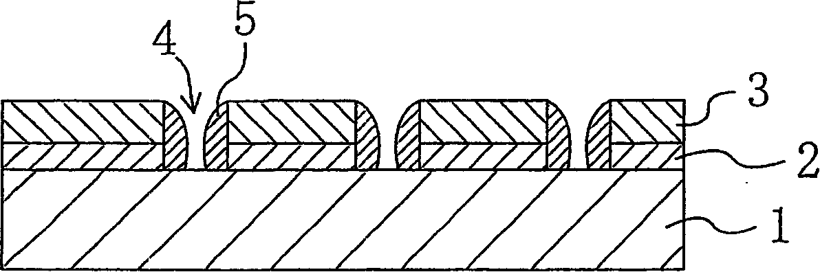
[0134] Figure 2A ˜ FIG. 2F are cross-sectional views showing a step of forming an element isolation region in the manufacturing process of the solid-state imaging device according to the second embodiment.
[0135] In the manufacturing process of the solid-state imaging device of this embodiment, first, in Figure 2A In the shown steps, a liner insulating film 2 made of a silicon oxide film with a thickness of about 1 to 50 nm is formed on a semiconductor substrate 1 . On the liner insulating film 2, an oxidation resistant film 3 made of a silicon nitride film or the like with a thickness of about 50 to 400 nm is formed. Furthermore, on the oxidation-resistant film 3, a resist (not shown) having openings in predetermined regions is formed.
[0136] Then, by etching using the resist as a mask, opening 4 penetrating liner insulating film 2 and oxidation resistant film 3 and exposing a predetermined region in the upper surface of semiconductor substrate 1 is formed. After tha...
no. 3 Embodiment approach
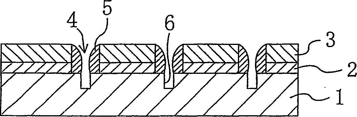
[0151] Figure 3A ~ Figure 3D It is a cross-sectional view showing a step of forming an element isolation region in the manufacturing process of the solid-state imaging device according to the third embodiment.
[0152] In the method of manufacturing the solid-state imaging device of this embodiment, first, in Figure 3A In the shown steps, a liner insulating film 2 made of a silicon oxide film with a thickness of about 1 to 50 nm is formed on a semiconductor substrate 1 . On the liner insulating film 2, an oxidation resistant film 3 made of a silicon nitride film or the like with a thickness of about 50 to 400 nm is formed. Furthermore, on the oxidation-resistant film 3, a resist (not shown) having openings in predetermined regions is formed.
[0153] Then, by etching using the resist as a mask, opening 4 penetrating liner insulating film 2 and oxidation resistant film 3 and exposing a predetermined region in the upper surface of semiconductor substrate 1 is formed. After ...
PUM
| Property | Measurement | Unit |
|---|---|---|
| Thickness | aaaaa | aaaaa |
| Thickness | aaaaa | aaaaa |
| Thickness | aaaaa | aaaaa |
Abstract
Description
Claims
Application Information