Zener diode and methods for fabricating and packaging same

A technology of Zener diode and manufacturing method, applied in semiconductor/solid-state device manufacturing, semiconductor devices, electrical components, etc., can solve problems such as reliability deterioration, increase Zener impedance, and reduce yield

Inactive Publication Date: 2006-08-02
LG ELECTRONICS INC
View PDF0 Cites 1 Cited by
  • Summary
  • Abstract
  • Description
  • Claims
  • Application Information

AI Technical Summary

Problems solved by technology

However, if a contact hole is formed in an undesired place through the contact hole forming process, a PN Zener diode or a resistive body is formed instead of a Zener diode having a bidirectional threshold voltage characteristic, thereby reducing its yield.
[0021] There is another problem: the current has to flow through a long diffusion layer, which increases the zener impedance, because the current flows from the electrode line to the diffusion layer and the substrate, and through another diffusion layer and another electrode Wire
[0022] There are additional problems: the limitation of the contact hole formation process causes the diffusion layer not to contact the electrode line, and the diffusion layer and the electrode line are not self-aligned resulting in deterioration of reliability
[0023] There are other problems: If the contact hole is formed by dry etching, the dry etching method will damage the diffusion layer, resulting in deterioration of Zener diode characteristics
[0033] There is a problem in the process according to this prior art that although there is no evaporation process of the inner layer insulating film, the film whose properties are changed at the diffusion mask used as the inner layer insulating film becomes to cause generation at the electrode line. causes of leakage current, and degrades the characteristics
[0034] There is another problem that the current flows through the long diffusion layer depicted in the manufacturing method of Fig. 1, thereby increasing the Zener resistance value, and if the contact hole is formed by dry etching, the dry etching method will destroy the diffusion layer. layer, resulting in deterioration of Zener diode characteristics

Method used


Image

  • Zener diode and methods for fabricating and packaging same
  • Zener diode and methods for fabricating and packaging same
  • Zener diode and methods for fabricating and packaging same

Examples


Embodiment Construction

[0055] Hereinafter, a zener diode and methods of manufacturing and packaging thereof according to preferred embodiments of the present invention will be described in detail with reference to the accompanying drawings.

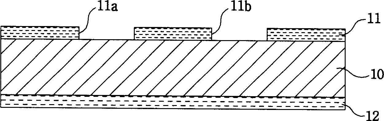
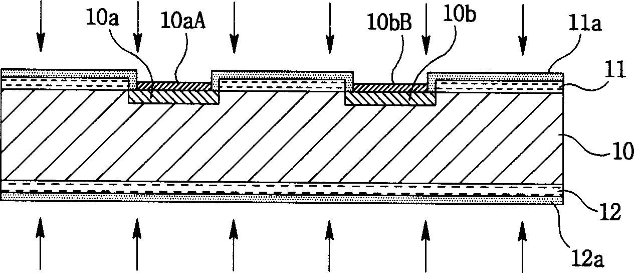
[0056] Figures 4a to 4d Shown is a sectional view of a Zener diode manufacturing process according to a first embodiment of the present invention, wherein upper and lower insulating films 110, 120 are formed on upper and lower portions of a substrate 100 having a first polarity, and the upper and lower mask layers 130, 140 are formed on the upper and lower insulating layers 110, 120, and a part of the upper mask layer 130 and the upper insulating film 110 is etched to form a pair of openings 135a, 135b through which, The substrate 100 is exposed. ( Figure 4a )

[0057] Preferably, the substrate 100 is a silicon substrate.

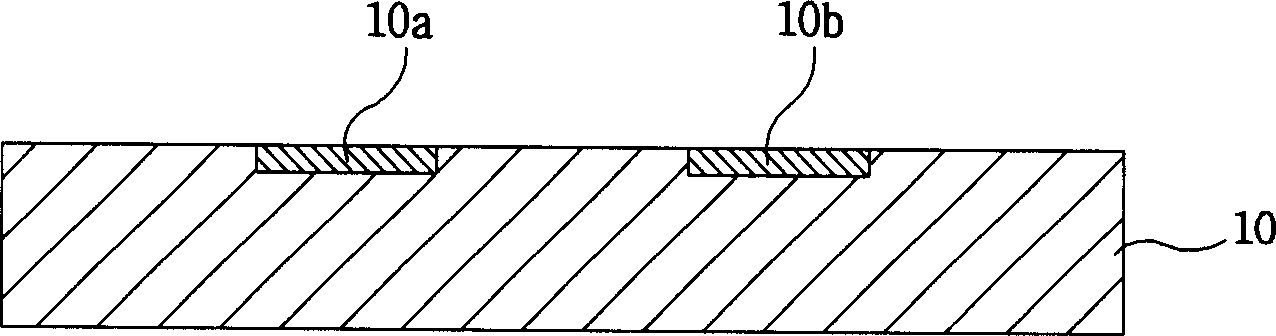
[0058] Next, the diffusion process is performed by introducing impurities having a second polarity opposite to the first polarity to ...


PUM


Abstract

A zener diode and methods for fabricating and packaging same are disclosed, whereby contact hole forming process exposing a diffusion layer is removed to enable to simplify the fabricating process, and the diffusion length not contacting the electrode line is determined by the crosswise length toward which the impurity is diffused to enable to reduce the zener impedance value. Furthermore, wet etching is used following the diffusion to remove the diffusion masks such that no damage is given to the diffusion layers to thereby enable to improve the zener diode characteristics.

Description

technical field [0001] This document relates to Zener diodes and methods of manufacturing and packaging them. Background technique [0002] Generally, there is a defect in devices with low-voltage impedance other than semiconductor devices that their life is shortened due to static electricity or surge voltage generated during measurement or packaging. As a protective device against low voltage impedance, Zener diodes are employed. [0003] A Zener diode is a diode that uses a reverse breakdown voltage, and the reverse breakdown of a PN Zener diode includes Zener breakdown that occurs at a low threshold voltage and avalanche breakdown that occurs at a higher threshold voltage. [0004] Zener breakdown is designed in such a way that if a high concentration of impurities is introduced into the semiconductor layer, a charge depletion layer of narrow width is formed, resulting in a high electric field even at a low voltage. [0005] In other words, if a high-concentration impu...

Claims


Application Information

Patent Timeline
IPC IPC(8): H01L21/329H01L21/60H01L29/866H01L25/16
CPCH01L2224/48137H01L2224/48091H01L2224/73265H01L2924/3011H01L2924/00H01L2924/00014H01L29/866
Inventor 宋基彰金根扈
Owner LG ELECTRONICS INC
Why Eureka
Try Eureka