Achieving method for multi-valued phase changing storage device

A technology of phase-change memory and multi-value storage, which is applied in the field of microelectronics to achieve multi-plant storage, reduce the erasing and writing current, and solve the problem of large peripheral circuits

Inactive Publication Date: 2006-08-02
FUDAN UNIV +1
View PDF0 Cites 6 Cited by
  • Summary
  • Abstract
  • Description
  • Claims
  • Application Information

AI Technical Summary

Problems solved by technology

The general solution is to reduce the write operation current by reducing the size of the memory cell, but there is no very effective solution to reduce the peripheral circuit

Method used


Image

  • Achieving method for multi-valued phase changing storage device
  • Achieving method for multi-valued phase changing storage device
  • Achieving method for multi-valued phase changing storage device

Examples


Embodiment 1

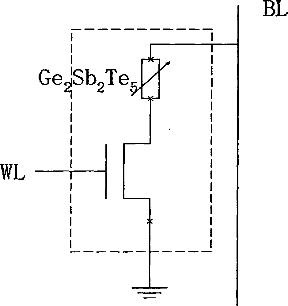
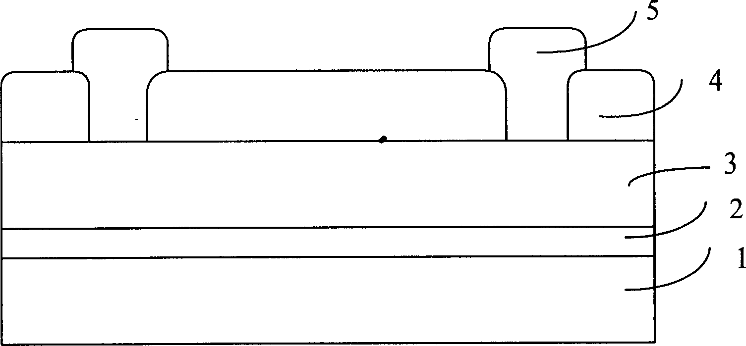
[0030] image 3 It is a structure of the present invention, wherein the gate electrode 1 is low-resistance n-type silicon, the high-resistance dielectric layer 2 is aluminum oxide (or silicon oxide, zirconium oxide, etc.), and 3 is amorphous Ge 2 Sb 2 Te 5 , The source and drain electrodes 5 are tungsten.

[0031] Figure 4 , 6 , 8 and 10 are the "read" operation process of the thin film transistor multi-value phase change memory. Figure 4 It is a schematic diagram of the “read” operation in the initial state of the thin film transistor: when a voltage higher than the threshold voltage is applied to the gate electrode 1, aluminum oxide and amorphous Ge 2 Sb 2 Te 5 The contact interface produces a carrier channel. Under the action of the source and drain electric fields, the carriers move in the channel to form a current. Obviously, the carrier channel length is the longest at this time, which is the distance between the two electrodes.

[0032] by Figure 5 , 7 And 9 write oper...

Embodiment 2

[0037] Figure 14 It is another specific implementation structure of the present invention. Among them, the gate electrode 1 is low-resistance n-type silicon, the high-resistance dielectric layer 2 is aluminum oxide (or silicon oxide, zirconium oxide, etc.), and 3 is amorphous Ge 2 Sb 2 Te 5 , The source and drain electrodes 5 are tungsten. When performing a "read" operation, a voltage higher than the threshold voltage is applied to the gate electrode 1. Aluminum oxide 2 and amorphous Ge 2 Sb 2 Te 5 A carrier channel is generated on the contact interface. Under the action of the source and drain electric field, the carrier moves in the channel to form a current, such as Figure 16 . When the “write” operation is performed, the source and drain tungsten electrodes 5 are grounded, and a programming voltage pulse is applied to the gate electrode 1. The aluminum oxide heats the Ge 2 Sb 2 Te 5 Crystallize or return it to an amorphous state to achieve non-volatile storage, seeFigure 15...

Embodiment 3

[0039] Figure 17 It is also a specific implementation structure of the present invention. Among them, the gate electrode 1 is low-resistance n-type silicon, the high-resistance dielectric layer 2 is aluminum oxide (or silicon oxide, zirconium oxide, etc.), and 3 is amorphous Ge 2 Sb 2 Te 5 , The source and drain electrodes 5 are tungsten, 7 is aluminum oxide (or silicon oxide, zirconium oxide, amorphous carbon, etc.), and 8 is a tungsten bottom electrode. When performing a "read" operation, a voltage higher than the threshold voltage is applied to the gate electrode 1. Aluminum oxide and amorphous Ge 2 Sb 2 Te 5 A carrier channel is generated on the contact interface. Under the action of the source and drain electric field, the carrier moves in the channel to form a current, such as Figure 19 . When the “write” operation is performed, the common electrode 8 is grounded, and a programming voltage pulse is applied to the source and drain electrodes 5, and the aluminum oxide 7 hea...


PUM


Abstract

This invention belongs to the field of microelectronic technology. It is a kind of method of multi-valued phase transformation memorizer. It uses semiconductor characters of phase transformation membrane material or composite material of other semiconductor material and phase transformation membrane to form semiconductor membrane transistor. It uses characters that phase transformation material can change reversibly under electricity effect to change channeling length of semiconductor membrane transistor so as to achieving storing long number in single memory cell. The membrane transistor can form spatial stereoscopic structure to increase density and do not need to occupy area of silicon substrate. Such, this invention can increase storing density greatly and solve the question of 1T1R structure phase transformation memorizer peripheral circuit occupying too large areas of silicon substrate.

Description

Technical field [0001] The invention specifically relates to a method for realizing a multi-value phase change memory, which belongs to the technical field of microelectronics. Background technique [0002] Phase Change Memory (Phase Change Memory-PCM), as a new generation of non-volatile memory, has many advantages such as: non-volatile, large number of reads and writes, long-term data retention, and high conversion / erasing speed. In terms of manufacturing cost, phase change memory also has significant advantages. [0003] The phase change memory generally uses chalcogenide compounds, such as Ge2Sb2Te5 alloy (hereinafter referred to as GST). Under the action of energy in the form of electricity or heat, the material can undergo a reversible transformation between polycrystalline and amorphous phases. Correspondingly, the resistance changes reversibly between low resistance and high resistance, which can be used to store information 1 or 0 . The current phase change memory cell g...

Claims


Application Information

Patent Timeline
Patent Type & Authority Applications(China)
IPC IPC(8): H01L29/78H01L29/02
Inventor 林殷茵蔡燕飞廖菲菲汤庭鳌陈邦明
Owner FUDAN UNIV
Why Eureka
Try Eureka