Optical sensor for thin film detection

An optical sensor and thin-film technology, applied in the field of optics, can solve problems such as inability to detect stress and growth rate in local areas of thin films, and high requirements for daily debugging and maintenance of optical systems, so as to enhance scientificity and accuracy, improve quality and output, Realize the effect of industrial scale production

Inactive Publication Date: 2006-08-23
XIDIAN UNIV
View PDF0 Cites 24 Cited by
  • Summary
  • Abstract
  • Description
  • Claims
  • Application Information

AI Technical Summary

Problems solved by technology

There are two shortcomings in this on-site film stress detection system: one is that the two laser beams must be strictly focused, which requires too high requirements for the design, installation, daily debugging and maintenance of the optical system

Method used


Image

  • Optical sensor for thin film detection
  • Optical sensor for thin film detection
  • Optical sensor for thin film detection

Examples


Embodiment Construction

[0030] The present invention will be described in further detail below with reference to the accompanying drawings.

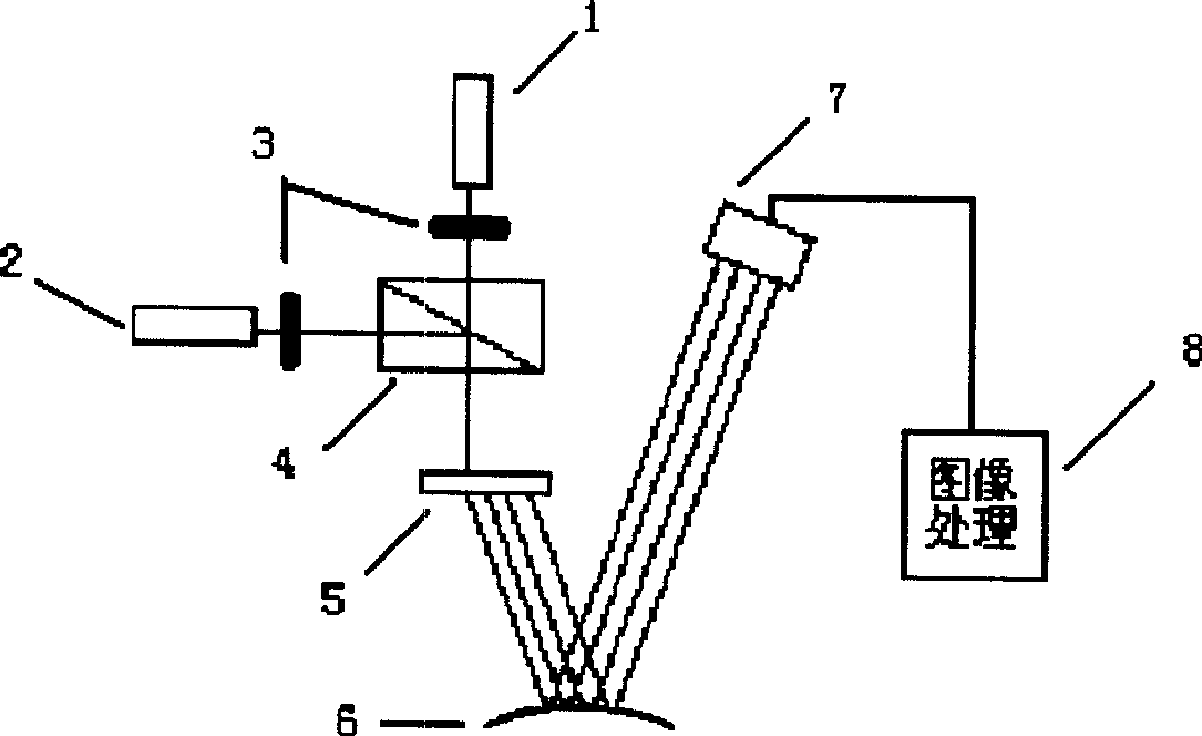
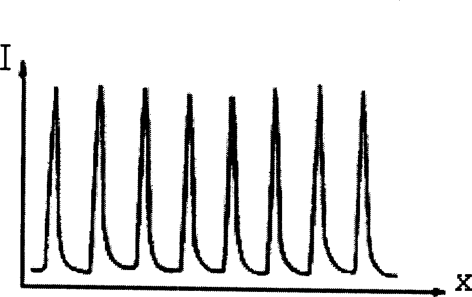
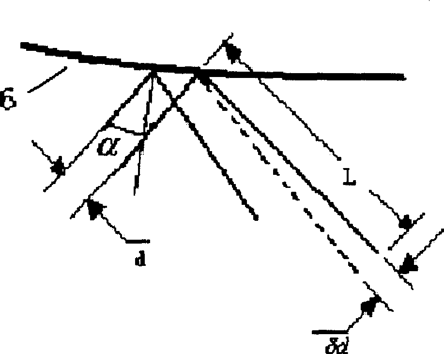
[0031] refer to figure 1 , the optical sensor of the present invention is composed of a first laser 1 , a second laser 2 , a controllable chopper 3 , a beam splitting prism 4 and a binary beam splitter 5 . The chopper (3) is controlled by an external circuit, so that the two laser beams of different frequencies output by the first pumping diode laser (1) and the second pumping diode laser (2) alternately pass through the chopper, and finally only Output a beam of laser light into the beam splitting prism (4). The binary grating beam splitter (5) is composed of a two-dimensional Dammann grating and a Fresnel zone plate, and is used to generate a self-converging multi-beam array. The present invention adopts the structure of two-color light incident and controllable optical chopper, can obtain Figure 4 The reflectance variation curve of light at two different...


PUM


Abstract

This invention discloses an optical sensor composed of pump diode lasers, a chopper and a beam splitter prism, in which, the first pump diode laser and the second pump diode laser output two beams of laser of different frequencies and output a beam laser by regulation of the chopper to irradiate on a dual grid splitter to form a 2-D beam array to be reflected on a CCD focal plane and imaged by a film sample to display the light spot position distribution information and the light intensity variety information of each spot of the reflection beam array to get the growing rate of the film by computing the transformation information of said light intensity, evaluate the film stress by beam offset information and Stoney equation and evaluate components of the material based on the incident light vacuum wavelength lambda< 0 > put forward by Brunner and function of the Al component x.

Description

technical field [0001] The invention belongs to the field of optical technology and relates to film detection, in particular to an optical sensor for detecting film growth rate and stress. Background technique [0002] It is well known in the industry that because stress changes in the film manufacturing process may cause the internal connection failure and delamination of the film to degrade the product quality, it is of great significance to control the degree of deformation of the film during the manufacturing process. Modern semiconductor processing requires electronic and optoelectronic equipment to precisely control the deposition process of thin film materials. At present, most processing processes need to measure parameters such as gas flow rate, deposition chamber pressure, and growth environment temperature in order to control the deposition process of thin film materials. . These parameters are generally preset empirical parameters for growing a film with a certa...

Claims


Application Information

Patent Timeline
IPC IPC(8): G01N21/00G01L1/24G06F19/00
Inventor 林晓春
Owner XIDIAN UNIV
Why Eureka
Try Eureka