Grid and formation of fast-flashing memory therewith

A memory and gate technology, which is applied in the field of gate and flash memory formation, can solve problems such as complex processes, and achieve the effects of increasing gate width, avoiding corners, and preventing erosion

Inactive Publication Date: 2006-11-01
POWERCHIP SEMICON CORP
View PDF0 Cites 8 Cited by
  • Summary
  • Abstract
  • Description
  • Claims
  • Application Information

AI Technical Summary

Problems solved by technology

However, performing a chemical mechanical polishing process (CMP) complicates the process

Method used


Image

  • Grid and formation of fast-flashing memory therewith
  • Grid and formation of fast-flashing memory therewith
  • Grid and formation of fast-flashing memory therewith

Examples


Embodiment Construction

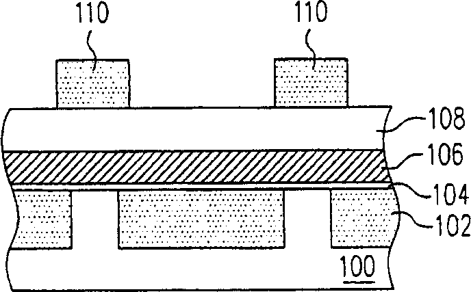
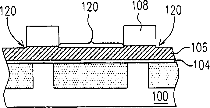
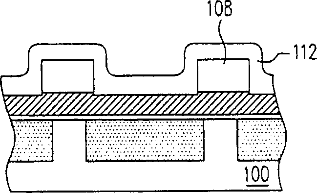
[0045] Figure 3A to Figure 3F is a schematic cross-sectional view of the manufacturing process of the gate according to a preferred embodiment of the present invention. Please refer to Figure 3A , a substrate 300 is provided, on which a gate dielectric layer 304 has been formed, and an isolation structure 302, such as a shallow trench isolation structure (STI), is provided in the substrate 300 . Then, a conductive layer 306 is formed on the gate dielectric layer 304, and its material is, for example, a doped polysilicon layer or other suitable materials. Next, an isolation protection layer 320 is formed on the conductor layer 306, such as a silicon oxide layer formed using tetraethoxysilane (TEOS) as a reactive gas source, and the method for forming this isolation protection layer 320 is, for example, low pressure chemical vapor deposition method. Afterwards, a sacrificial layer 308 is formed on the isolation protection layer 320 , wherein the sacrificial layer 308 is, fo...


PUM


Abstract

The method comprises: orderly forming a grid dielectric layer, a conducting layer, an isolation protective layer, a sacrificial layer and a patterned mask layer on a substrate; using the patterned mask layer as etching mask and using the isolation protective layer as etching stop layer to remove the exposed sacrificial layer, and then removing the patterned mask layer; forming a spacer on the sidewall of the sacrificial layer, and then using the spacer and the sacrificial layer as etching mask to remove the portion of isolation protective layer and conducting layer in order to form a grid; finally removing the sacrificial layer, spacer and isolation protective layer. The invention can avoid generation of edge and corner on the top surface of grid at the time of etching sacrificial layer.

Description

technical field [0001] The invention relates to a method for forming a semiconductor element, in particular to a method for forming a gate and a flash memory. Background technique [0002] With the continuous miniaturization of semiconductor components, the demand for how to improve the integration of components is becoming more and more urgent. Among them, the critical dimension of the semiconductor element is usually limited by the resolution of the lithography process, and the resolution of the lithography process depends on the wavelength of the light source (wavelength), so this will limit the pattern pitch of the semiconductor element to a fixed distance superior. If the distance between the patterns is smaller than the wavelength of the light source, it cannot be precisely patterned and defined. [0003] Therefore, a process that can increase the gate width to reduce the gate pitch has been developed, such as Figure 1A to Figure 1E shown. [0004] Figure 1A to Fi...

Claims


Application Information

Patent Timeline
Patent Type & Authority Applications(China)
IPC IPC(8): H01L21/28H01L21/44H01L21/8234H01L21/8246H01L21/8247
Inventor 刘振强宋达童心颖
Owner POWERCHIP SEMICON CORP
Why Eureka
Try Eureka