Non-volatile memory device

A storage device and charge trapping technology, applied in information storage, static memory, read-only memory, etc., can solve problems such as channel tunneling and changing the threshold voltage of transistors

Inactive Publication Date: 2006-11-15
MASSACHUSETTS INST OF TECH
View PDF5 Cites 11 Cited by
  • Summary
  • Abstract
  • Description
  • Claims
  • Application Information

AI Technical Summary

Problems solved by technology

Injecting charge into the material can cause channel tunneling, which can change the transistor's threshold voltage

Method used


Image

  • Non-volatile memory device
  • Non-volatile memory device
  • Non-volatile memory device

Examples


Embodiment Construction

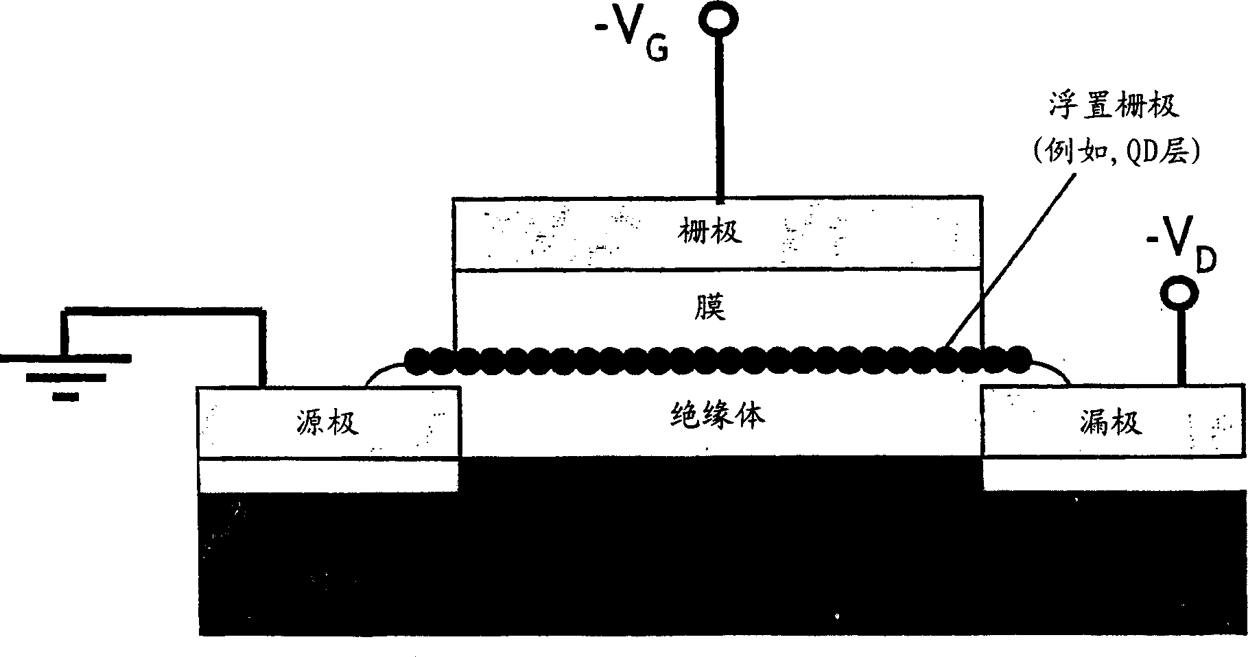
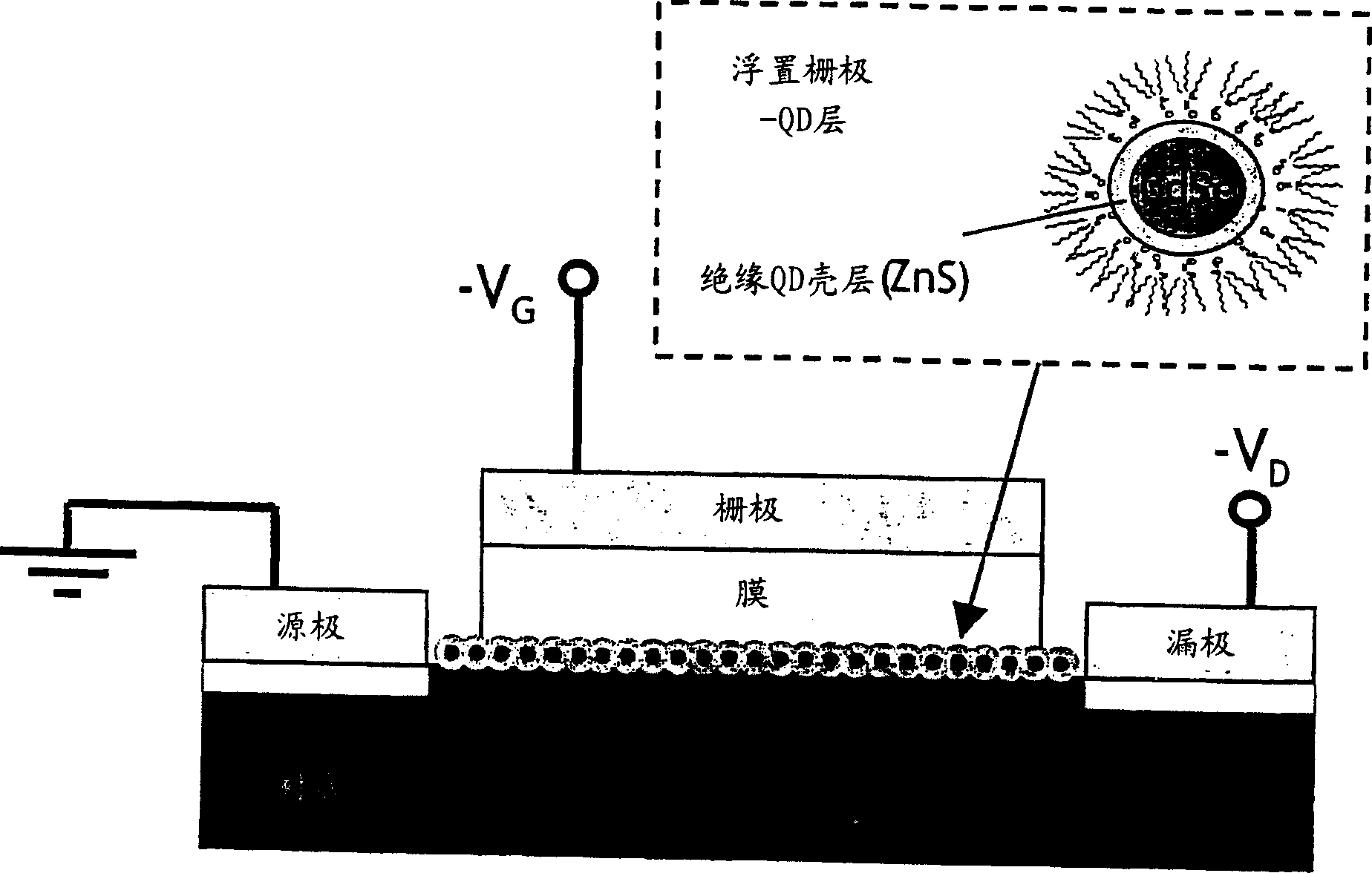
[0024] The memory device may include a room temperature integrable memory element. Memory elements can be used in a variety of electronic technology platforms, including organic, III-V, and even silicon electronics. The memory element may be a non-volatile memory device comprising a layer of charge-trapping material with selectable lateral conductance, such as nanoparticles with a selectable outer layer. Memory elements can be fabricated using room temperature methodologies to form hybrid organic / inorganic devices.

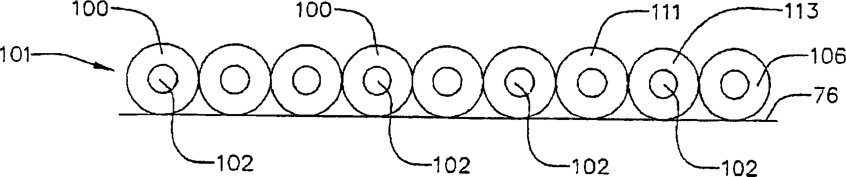
[0025] The memory element may be an array of chip-scale memory cells. Chip-scale memory cell arrays can be formed by exploiting the charge-trapping properties of nanoparticle monolayers. Single memory cell configurations include field effect transistor structures in which nanoparticles make up the floating gate. An example of such a structure is shown in figure 1 . This device is similar to other devices based on other materials, but has many advantages over ...


PUM


Abstract

A memory device can include an active layer that has a selectable lateral conductivity. The layer can include a plurality of nanoparticles.

Description

[0001] This application claims the benefit of US Application No. 60 / 508,272, filed October 6, 2003, which is incorporated by reference in its entirety. [0002] This invention was made with government support under Contract No. DMR-9400334 of the National Science Foundation. The government may have certain rights in the invention. technical field [0003] The invention relates to a nonvolatile memory device. Background technique [0004] Non-volatile memory is a component of an increasing number of portable products. A nonvolatile floating gate memory device may include a gate of a metal oxide semiconductor field effect transistor (MOSFET). The memory operation of field effect transistors relies on the storage of charge by the materials used to form the active portion of the device. In these floating gate memory devices, the material of the active portion of the device acts as a charge storage element within the gate oxide of the MOSFET. Injecting charge into the materia...

Claims


Application Information

Patent Timeline
Patent Type & Authority Applications(China)
IPC IPC(8): H01L21/336G11C13/02G11C16/04H01LH01L21/28H01L29/423H01L29/788H01L29/80H01L31/0336
CPCB82Y10/00B82Y30/00G11C13/02G11C16/0466G11C2213/12G11C2213/18G11C2213/53G11C2216/06H01L29/127H01L29/2203H01L29/42332H01L29/7881H01L29/40114
Inventor 芒吉·G·鲍温迪弗拉迪米尔·布洛维克塞思·A·科
Owner MASSACHUSETTS INST OF TECH
Why Eureka
Try Eureka