Non-volatile semiconductor memory device

A storage device, non-volatile technology, used in semiconductor devices, semiconductor/solid-state device manufacturing, read-only memory, etc., can solve problems such as insufficient data "0" writing

Active Publication Date: 2006-11-29
KIOXIA CORP +1
View PDF0 Cites 4 Cited by
  • Summary
  • Abstract
  • Description
  • Claims
  • Application Information

AI Technical Summary

Problems solved by technology

That is, the threshold value of the memory cell has a tolerance to 0V, and if it is not 0.5V or more, a current flows in the selected memory cell, and it is detected that data "0" is not written enough

Method used


Image

  • Non-volatile semiconductor memory device
  • Non-volatile semiconductor memory device
  • Non-volatile semiconductor memory device

Examples


Embodiment 1

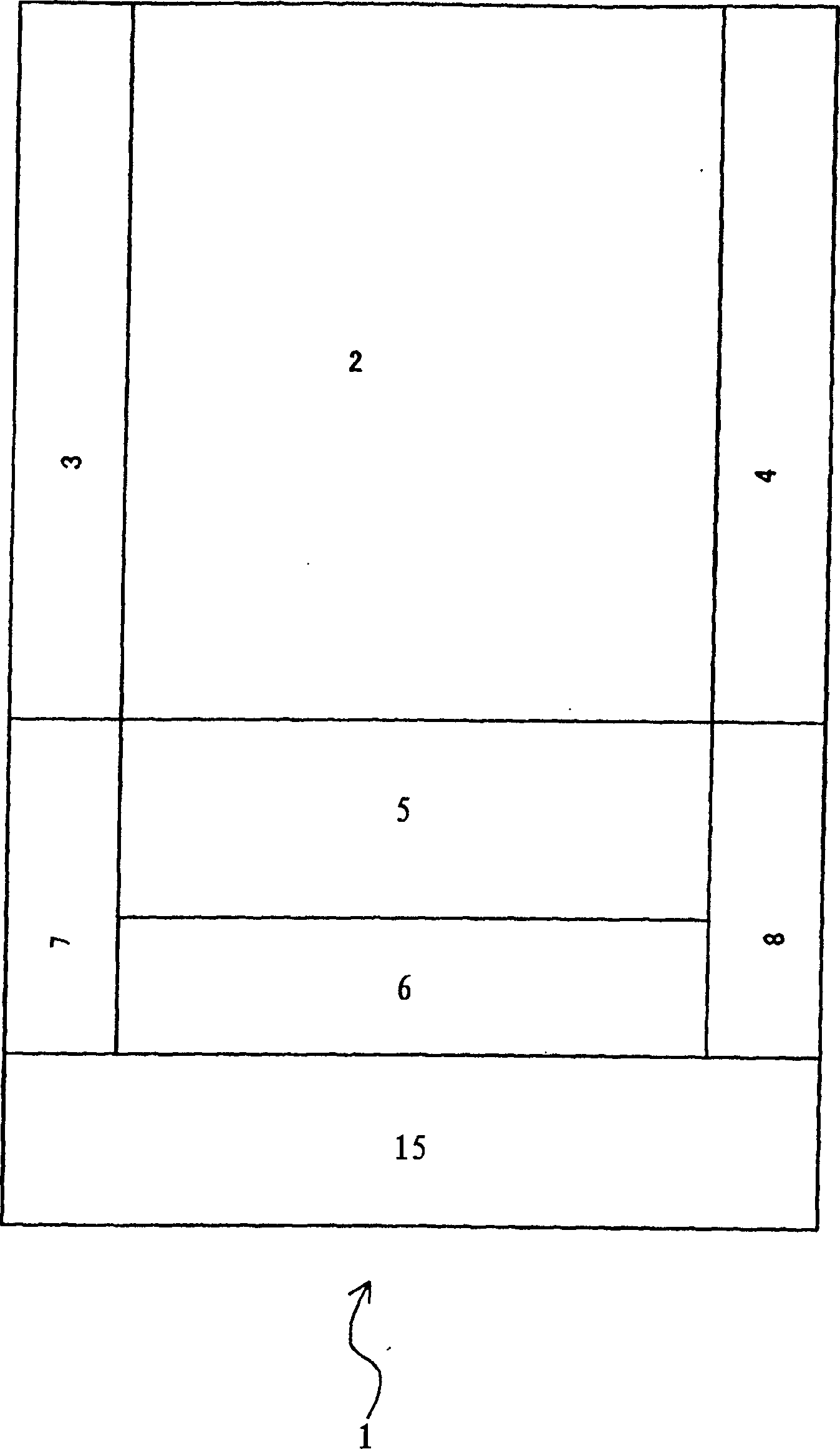
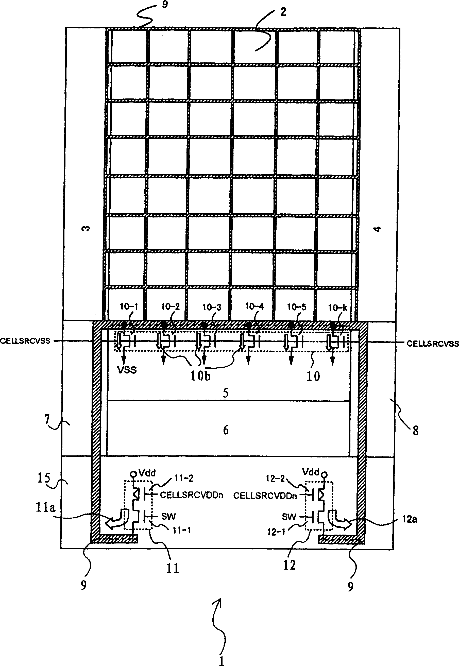
[0097] In this embodiment, an example in which charging cell source line drivers 11 and 12 are arranged on intersections 7 and 8 in NAND flash memory 1 of the present invention described in the above embodiments will be described.

[0098] refer to Figure 5 . Figure 5 A schematic configuration diagram of the NAND-type flash memory 20 of the present invention according to the present embodiment is shown. right in Figure 5 In the NAND type flash memory 20 according to the present invention shown in this embodiment, the same configuration as that of the NAND type flash memory 1 of the present invention described in the above-mentioned embodiment is given the same reference numerals, so it will not be omitted here. Let me explain.

[0099] Such as Figure 5 As shown, in the NAND flash memory 20 of this embodiment, the cell source line drivers 11 and 12 for charging are disposed on the intersection portion 7 and the intersection portion 8, respectively. In this way, the wir...

Embodiment 2

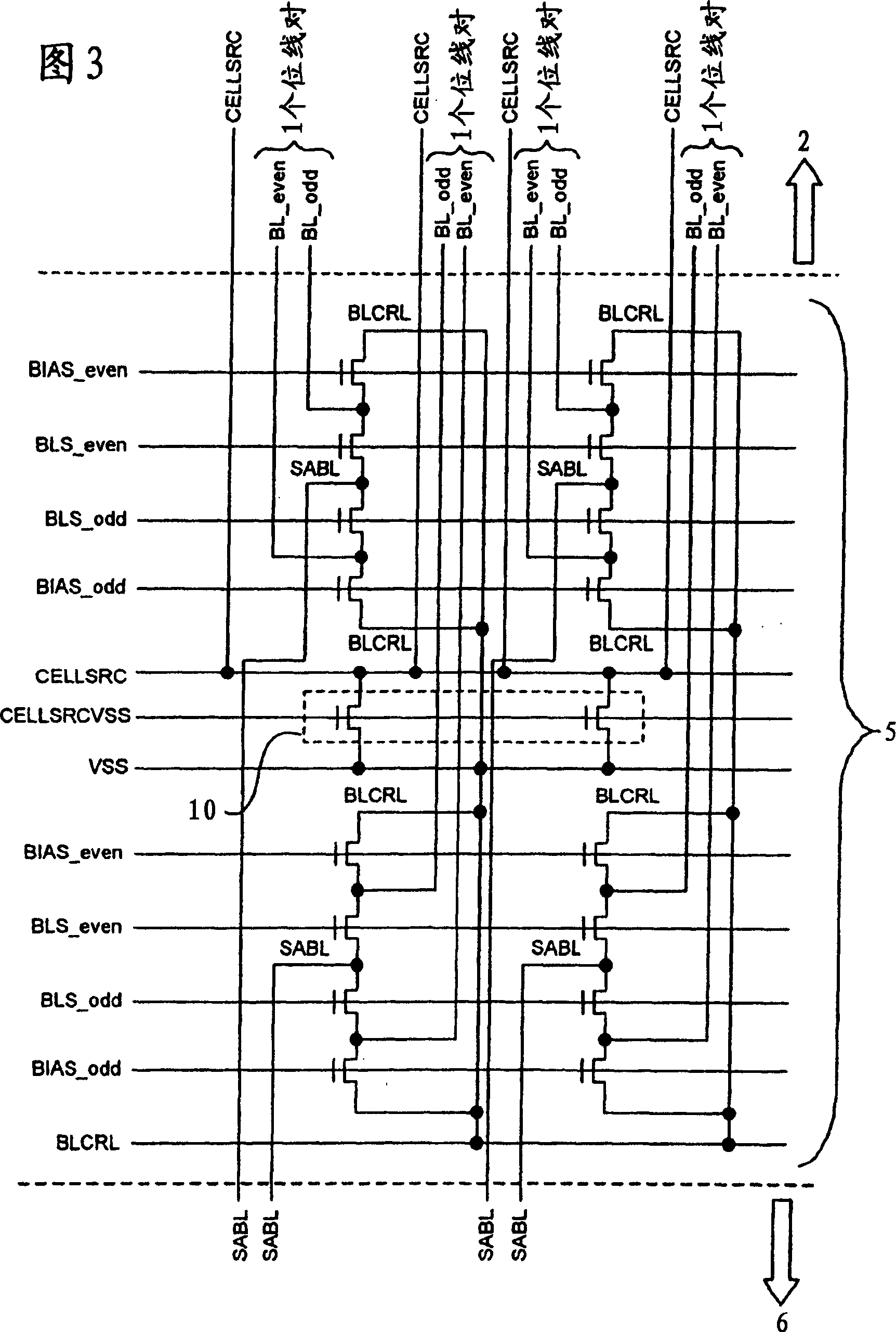
[0101] In this embodiment, in the NAND flash memory 1 of the present invention described in the above-mentioned embodiments, the cell source line (CELLSRC) is arranged in the high-voltage transistor region of the sense amplifier portion next to the cell array. An example of a transistor whose potential is equalized with that of the bit line shield line (BLCRL).

[0102] refer to Figure 6 . Figure 6 A schematic configuration diagram of the NAND-type flash memory 30 of the present invention according to the present embodiment is shown. right in Figure 6 In the NAND type flash memory 30 according to the present invention shown in this embodiment, the same configuration as that of the NAND type flash memory 1 of the present invention described in the above-mentioned embodiment is given the same reference numerals, so it will not be omitted here. Let me explain.

[0103] In the NAND flash memory 30 of this embodiment, the potential of the cell source line (CELLSRC) and the p...

Embodiment 3

[0116] This embodiment describes an example in which charging cell source line drivers 11 and 12 are arranged on intersections 7 and 8, respectively, in NAND flash memory 30 of the present invention described in Embodiment 2 above.

[0117] refer to Figure 12 . Figure 12 A schematic configuration diagram of the NAND type flash memory 40 of the present invention according to the present embodiment is shown. right in Figure 12 In the NAND flash memory 40 according to the present invention shown in this embodiment, the NAND flash memory 1 of the present invention and the NAND flash memory 30 of the present invention described in the above-mentioned embodiment mode and Example 2 are The same structures are given the same reference numerals, so they will not be described again here.

[0118] Such as Figure 12 As shown, in the NAND flash memory 40 of this embodiment, the cell source line drivers 11 and 12 for charging are disposed on the intersection portion 7 and the inters...


PUM


Abstract

According to one embodiment of this invention, a non-volatile semiconductor memory device of high speed program operation is realized. It provides a non-volatile semiconductor memory device comprising a cell array in which NAND strings having electrically re-programmable memory cells are connected in series are disposed in a matrix form; sense amplifiers for sensing threshold voltages of said memory cells by sensing potentials of bitlines connected to said memory cells and for having a first region having high voltage transistors and a second region having low voltage transistors; cell source lines connected to an end of said NAND strings; and a first cell source line driver being connected to said cell source lines and having a first transistor for supplying a grounding potential or a low potential to said cell source line, said first transistor of said cell source line driver being disposed in said first region of said sense amplifiers.

Description

technical field [0001] The present invention relates to an electrically rewritable semiconductor memory device. In particular, it relates to a NAND cell type EEPROM (NAND type flash memory) among nonvolatile semiconductor memory devices. Background technique [0002] In recent years, the demand for small and large-capacity non-volatile semiconductor memory devices has increased dramatically. Compared with the existing NOR flash memory, high integration can be realized by connecting multiple memory cells in series to form a NAND cell block. , Large-capacity NAND-type flash memory attracts attention. The data writing and erasing operations of the NAND flash memory are as follows. [0003] The data writing operation of the NAND flash memory is mainly performed sequentially from the memory cell farthest from the bit line. First, when the data write operation starts, 0V (write data "0") or power supply voltage Vcc (write data "1") is applied to the bit line corresponding to th...

Claims


Application Information

Patent Timeline
Patent Type & Authority Applications(China)
IPC IPC(8): H01L27/115G11C16/02
CPCG11C16/0483H10B99/00
Inventor 前岛洋
Owner KIOXIA CORP
Why Eureka
Try Eureka