Micro-thin pen for direct writing electronical photoelectronic component and its constituting device

A technology of optoelectronics and components, applied in the field of rapid manufacture of wires, resistors, micro-pen and devices composed of them, capacitors, inductors and optical waveguides, can solve the problem of small viscosity range of paste, few types of paste, electronic components The problem of limited types, etc., achieves the effect of short preparation time, fast wiring speed and low processing cost

Active Publication Date: 2007-01-03
WUHAN XINRUIDA LASER ENG
View PDF0 Cites 8 Cited by
  • Summary
  • Abstract
  • Description
  • Claims
  • Application Information

AI Technical Summary

Problems solved by technology

However, the biggest disadvantage of this technology is that the viscosity range of the slurry that can be atomized is too small, only 0.7-1000×10 -3 Between Pa and S, so there are fewer types of pastes that can be applied, and the types of electronic components that can be prepared are limited

Method used


Image

  • Micro-thin pen for direct writing electronical photoelectronic component and its constituting device
  • Micro-thin pen for direct writing electronical photoelectronic component and its constituting device
  • Micro-thin pen for direct writing electronical photoelectronic component and its constituting device

Examples


Embodiment 1

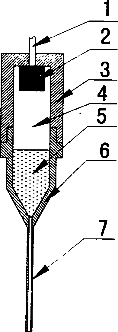
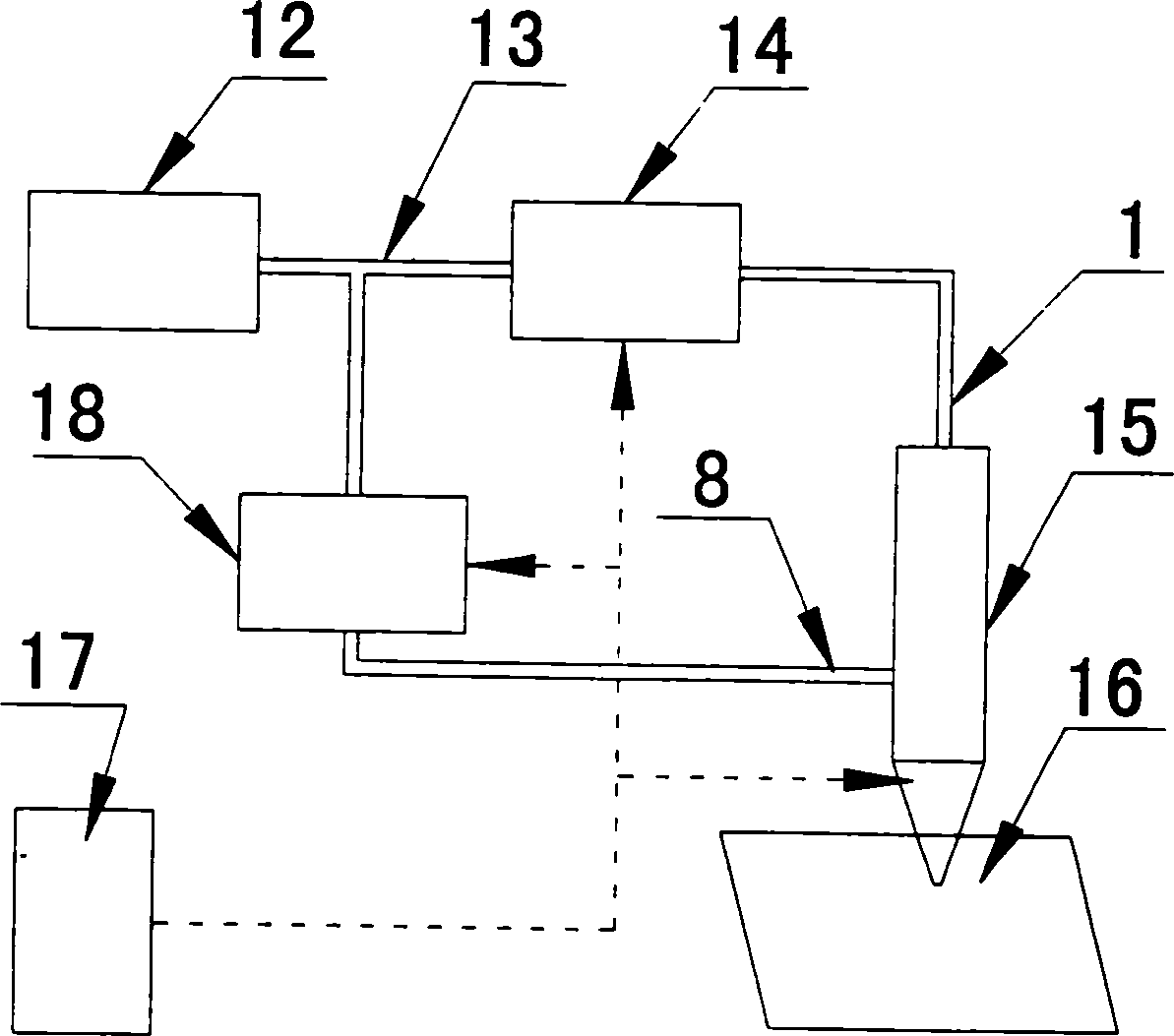
[0027] The composition of the whole fine pen direct writing device is as follows: Figure 4 shown. The first pressure control device 14 and the second pressure control device 18 have the same structure, the former is composed of a pressure regulating valve 25, a pressure gauge 26 and a solenoid valve 27 in series, and the latter is composed of a pressure regulating valve 31, a pressure gauge 30 and a solenoid valve 29 in series made. The compressed nitrogen gas source 19 is connected to the three-way pipe 24 through the gas source switch 20, the pressure gauge 21, the pressure regulating valve 22 and the pressure gauge 23 in sequence. The air pipe is connected with the pressure regulating valve 31. The substrate 16 is located on the workbench 28 , and the controller 17 controls the movement of the workbench 28 through a motor. Micro pen 15 adopts figure 1 In the structure shown, the inner diameter of the nib 7 is 120 μm. When in use, first turn on the gas source switch 20...

Embodiment 2

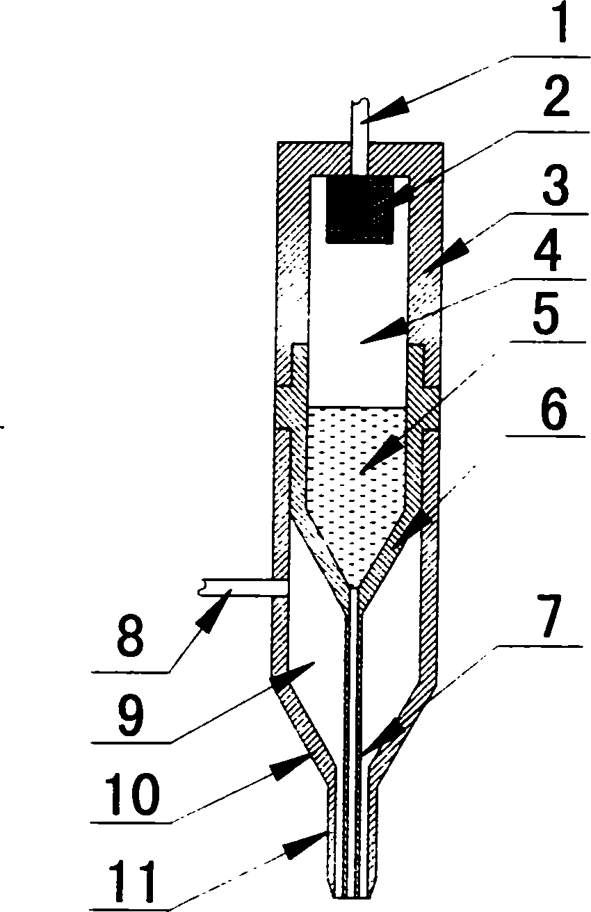
[0031] when according to figure 2 When the fine pen shown in the figure is used for jet direct writing, it needs to be turned on Figure 4 The second pressure control device 18 shown is the atomizing gas circuit. In jet direct writing, the inner diameter of the pen tip 7 is 120 μm, the outer diameter is 180 μm, and the gap between the pen tip 7 and the air nozzle 11 is 10 μm.

[0032] Using such a device structure can realize direct writing based on jetting principle. In direct writing, the slurry will be atomized first, and then deposited on the substrate, and different shapes can be obtained by controlling the movement of the worktable. When atomizing direct writing, the tip of the pen does not touch the substrate, so electronic components can be made on curved surfaces; at the same time, the atomization has a divergent effect on the slurry, and the resolution of the line width will decrease during direct writing, but when it needs to be It has advantages when writing di...

Embodiment 3

[0036] The device adopted is the same as in Example 1, and the operation mode and steps are the same as in Example 1. However, the electronic paste is replaced by a polymer with excellent performance, and the device can be used to write directly to the optical waveguide.

[0037] Adjust the air pressure and other parameters, set the control program, and after debugging the device, put fluorinated polyimide (PI) in the micro pen, start the device, and then write the optical waveguide on the silicon substrate, the waveguide width is about 100 microns , with a thickness of about 5 microns. The light-passing experiment is carried out on the prepared optical waveguide to test the loss of the optical waveguide, and the minimum loss can reach 0.5dB / cm, which can meet the manufacturing requirements of optoelectronic devices.


PUM


Abstract

The invention discloses a mini pen of direct-writing electronic/photoelectronic component and its structure. The decompression device is located in the cap of the pen and connected with the pressing pipe on the top of the cap. The lower end of the cap is connected airtightly and movably with the upper end of the brush stand to form the bunker used to deposit the material that needs to deposit. The lower end of the brush stand is penpoint. The mini pen links with the air supply by two shunt-wound press controlling devices. The controller controls two gas paths and the relative movement of the mini pen to the base to form the direct-writing device. The mini pen can be used to create the electronic component and the photoelectronic component, for example, the polymer filter waveguide. Depending on the structure and polymer character of the mini pen, the polymer material can be put into the mini pen and direct write the filter waveguide. The wiring speed is rapid; the span of the wire width is large; the cost of producing and operating is low. The wiring speed is between 2 and 15mm/s and the wire width is between 0.06 and 2mm.

Description

technical field [0001] The invention belongs to the field of electronic / optoelectronic components manufacturing, and in particular relates to a micropen for directly writing electronic / optoelectronic components and a device composed of the same. The invention is especially suitable for rapidly manufacturing wires, resistors, capacitors, inductors and optical waveguides. Background technique [0002] The emergence and development of large-scale integrated circuits have greatly increased the circuit density, and continue to develop in the direction of high precision, high density, thin lines, small holes, high reliability, low cost, and automated continuous production. Especially in recent years, with the continuous development of electronic products in the direction of integration, miniaturization, short timeliness, small batches, and multiple varieties, the factors that restrict the further improvement of the quality of electronic products have changed from the original chip...

Claims


Application Information

Patent Timeline
Patent Type & Authority Applications(China)
IPC IPC(8): H01L21/00H01L21/768H01L21/288H01L21/3205
Inventor 曾晓雁李祥友王泽敏李金洪王小宝曹宇
Owner WUHAN XINRUIDA LASER ENG
Why Eureka
Try Eureka