

Method and system for forming a film of material using plasmon assisted chemical reactions
A plasma and chemical reaction technology, applied in microstructure or nanostructure and its application fields, can solve the problems of film quality deterioration and achieve the effects of fast heat generation, high device yield, and good space control
- Summary
- Abstract
- Description
- Claims
- Application Information
AI Technical Summary
Problems solved by technology
Method used
Image

Examples
Embodiment
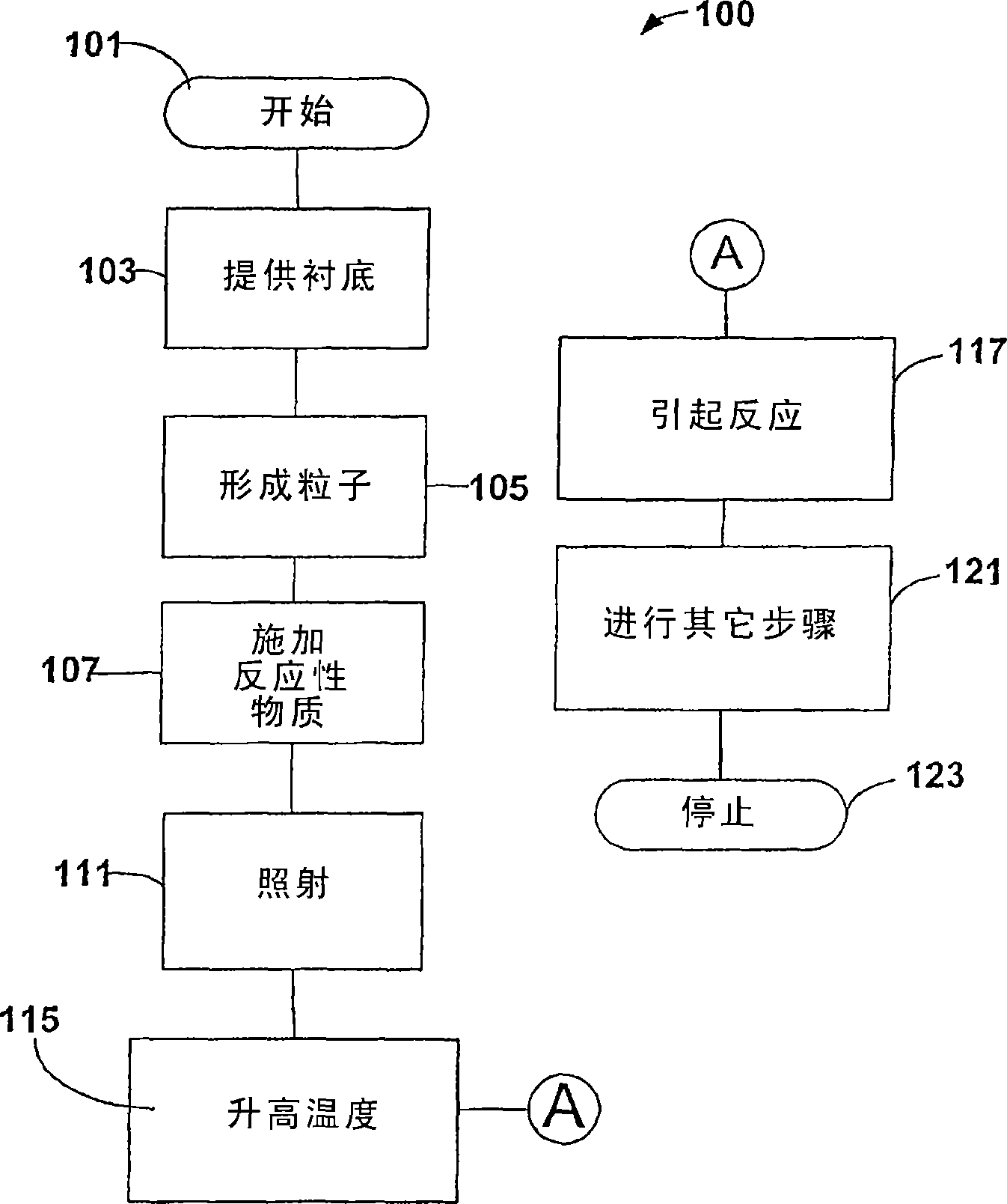
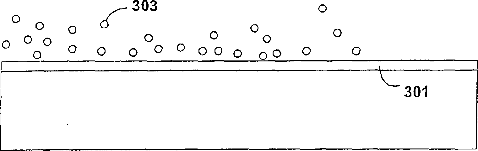
[0082] In order to demonstrate the principles and operation of the present invention, we provide examples of the present invention in a chemical vapor deposition environment. These examples are illustrative only, and should not limit the scope of the claims. Those of ordinary skill in the art would recognize many variations, improvements, and substitutions. As background information, we provide information on conventional chemical vapor deposition and its applications in relation to the methods and systems of the present invention. One of the goals of this CVD study is to achieve local control of nanostructures. Ferroelectric materials are ideal for non-volatile memory applications. However, challenges exist in fabricating uniform nanoscale arrays of ferroelectric materials. Conventional CVD is limited by only providing a random deposition process.
[0083] In this example, the localized heating of metallic nanostructures (such as particles, wires, or arrays thereof on a s...
PUM
 Abstract
Description
Claims
Application Information