Transistor with quantum dots in its tunnelling layer

A quantum dot and body technology, applied in the field of semiconductor components, can solve the problems of complex, expensive, difficult to manufacture tunnel oxide layers, etc., and achieve the effect of simplifying the manufacturing process and reducing the manufacturing cost

Inactive Publication Date: 2007-01-24
NXP BV
View PDF1 Cites 4 Cited by
  • Summary
  • Abstract
  • Description
  • Claims
  • Application Information

AI Technical Summary

Problems solved by technology

[0006] The disadvantage of this transistor is that it is very complex and expensive to manufacture using vacuum technology
Fabrication of tunnel oxide layers often creates more difficulties

Method used


Image

  • Transistor with quantum dots in its tunnelling layer

Examples


Embodiment 1

[0034] Example of Example 1

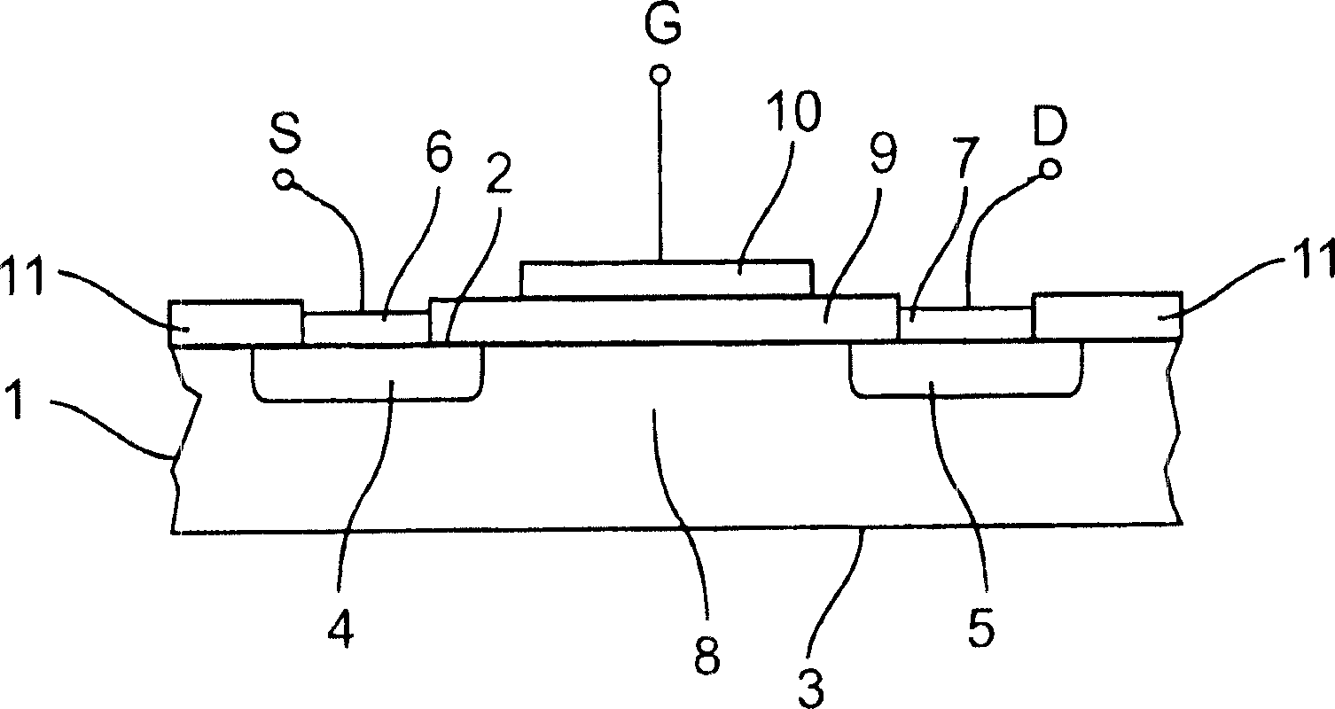
[0035] To produce the semiconductor component according to the invention, the n-conductive source region 4 and the n-conductive drain region 5 are first produced by ion-implanting phosphorous into the boron-doped silicon semiconductor body 1 . Then, by means of photolithography, source electrodes 6 and drain electrodes 7 made of Al doped with 0.5 wt. % Cu are applied. By spin coating will contain TiO 2 / SiO 2 A suspension of quantum dots is applied between the two electrodes 4, 5 and allowed to consolidate under an inert atmosphere at temperatures up to 300°C. The consolidated insulating layer 9 contains SiO embedded in 2 5 nm diameter TiO in the matrix 2 quantum dots. After cooling to room temperature, a gate electrode 10 of Al is applied to the insulating layer 9 .


PUM


Abstract

The invention describes a semiconductor component, which is arranged in a semiconductor body (1), with at least one source zone (4) and with at least one drain zone (5) of a first conductivity type in each case, with at least one body zone (8) of a second conductivity type arranged in each case between source zone and drain zone, and with at least one gate electrode (10) insulated relative to the semiconductor body by means of an insulating layer (9), the insulating layer (9) being a consolidated, preferably sintered, layer containing quantum dots. The invention further describes a method of producing such a semiconductor component wherein a dialectric suspension containing quantum dots is applied to a semiconductor body and then consolidated, for example by sintering.

Description

technical field [0001] The invention relates to a semiconductor component, which is arranged in a semiconductor body, in each case having at least one source region and at least one drain region of a first conductivity type, in each case arranged between the source region and the drain region There is at least one body region of the second conductivity type in between, and at least one gate electrode is insulated from the semiconductor body by means of an insulating layer. The invention also relates to a method of manufacturing a semiconductor component. Background technique [0002] Transistor-functional components are known in a wide variety of embodiments, one of which is of the Field Effect Transistor (FET) type. In the case of field effect transistors, the charge carrier density in the electronic channel, which is placed in contact with the source and drain regions, is changed by applying a voltage to the control electrode (gate electrode). The control electrode can p...

Claims


Application Information

Patent Timeline
Patent Type & Authority Applications(China)
IPC IPC(8): H01L29/792H01L21/336H01L21/8246H01L21/28H01L29/423
CPCH01L29/42332H01L21/28282H01L29/792H01L21/28273B82Y10/00H01L29/40114H01L29/40117
Inventor S·P·格拉波夫斯基C·R·隆达
Owner NXP BV
Why Eureka
Try Eureka