Controlling method for gate formation of semiconductor device

一种半导体、栅极的技术,应用在半导体装置的栅极形成控制领域,能够解决无法提供、很难完整设定等问题,达到生产量减少的效果

Inactive Publication Date: 2007-01-31
TAIWAN SEMICON MFG CO LTD
View PDF0 Cites 7 Cited by
  • Summary
  • Abstract
  • Description
  • Claims
  • Application Information

AI Technical Summary

Problems solved by technology

[0005] Although equipment can be used to determine the critical dimension and profile of the gate of the device, this device generally cannot provide immediate response to the photolithography process to reduce variation, and the traditional inspection results are generally not used to adjust the subsequent etching process
In addition, due to process variations, gate critical dimensions and profile will be affected by factors unknown to the designer, making it difficult to obtain a complete set of process control

Method used


Image

  • Controlling method for gate formation of semiconductor device
  • Controlling method for gate formation of semiconductor device
  • Controlling method for gate formation of semiconductor device

Examples


Embodiment Construction

[0035] In order to make the above objects, features and advantages of the present invention more comprehensible, a preferred embodiment will be described in detail below together with the accompanying drawings.

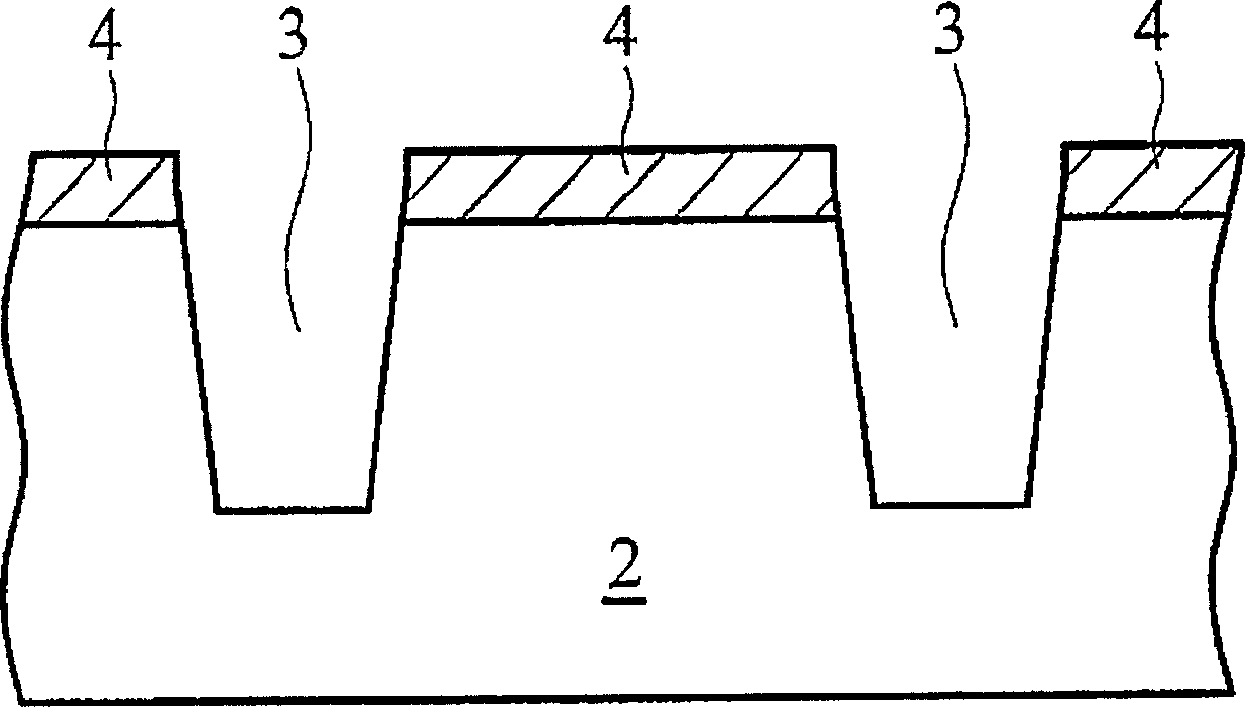
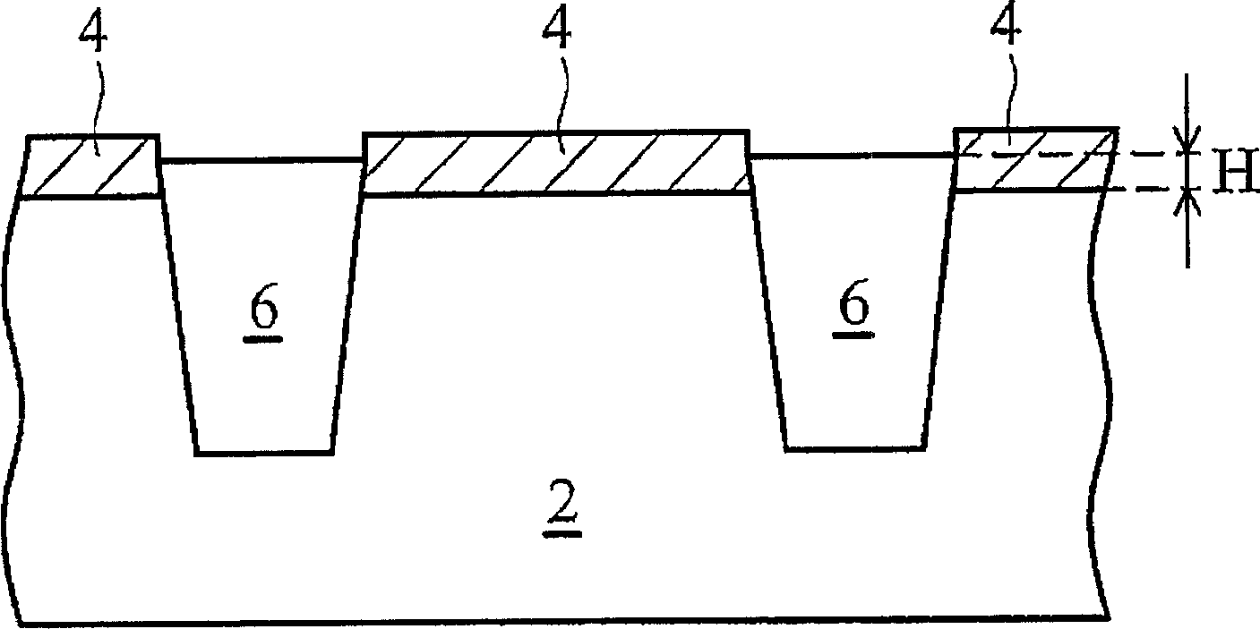
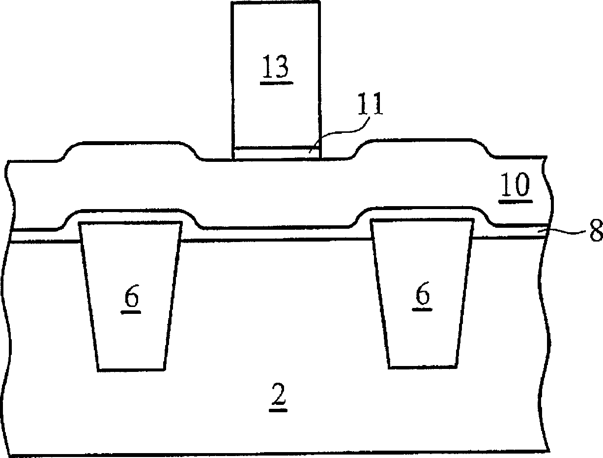
[0036] figure 1 , figure 2 , Figure 3A to Figure 3C ,as well as Figure 4It represents a general MOS device and its formation, including the formation of shallow trench isolation (Shallow Trench Isolation, STI) 6 . A mask layer 4 is formed on the active region 2 . In the provided embodiment, the mask layer 4 is formed of silicon nitride using Low Pressure Chemical Vapor Deposition (LPCVD). In other embodiments, the mask layer 4 is formed by thermal nitridation of silicon, plasma-assisted chemical vapor deposition (Plasma Enhanced Chemical Vapor Deposition, PECVD), or plasma anodic nitridation using nitrogen-hydrogen ( plasmaa nodicnitridation) to form. The channel 3 is formed by anisotropically etching into the active region 2 through the mask layer 4 or silic...


PUM


Abstract

A method of controlling gate formation of semiconductor devices includes determining the correlation between the step heights of isolation structures and the over-etching time by measuring step heights of isolation structures, determining an over-etching time based on the step heights, and etching gates using the over-etching time. The method may include an after-etching-inspection to measure the gate profile and fine-tune the gate formation control. Within-wafer uniformity can also be improved by measuring the step height uniformity on a wafer and adjusting gate formation processes. The invention provides a simple and economic method and system of controlling gate formation of semiconductor devices. The method control the gate, as well as not leading to a notable decrease in production.

Description

technical field [0001] The present invention relates to the manufacturing process of semiconductor devices, in particular to the gate formation control of semiconductor devices. Background technique [0002] Current demands for high density and high performance in ultra-scale integrated circuits require sub-micron components, increased transistor and circuit speed, and improved reliability. These demands require the formation of device elements with high precision and consistency. While these device elements are still in the form of semiconductor wafers, then careful process monitoring is required, including device frequency and detailed inspection. [0003] When the design rules shrink and the process window (such as the limit of error in the process) becomes smaller, the inspection and determination of the critical dimension (Critical Dimension, CD) of the surface element and its cross-sectional shape (profile) become more and more important . Wherein, the critical dime...

Claims


Application Information

Patent Timeline
Patent Type & Authority Applications(China)
IPC IPC(8): H01L21/28H01L21/335H01L21/66
CPCH01L22/26H01L22/12H01L21/28123H01L21/76224H01L2924/0002H01L2924/00
Inventor 左佳聪赖俊宏吴玫真许立德苏斌嘉陈柏仁
Owner TAIWAN SEMICON MFG CO LTD
Why Eureka
Try Eureka