White light organic electroluminescent device
A technology of electroluminescent devices and phosphorescent luminescent materials, applied in the direction of electric solid devices, electrical components, semiconductor devices, etc., can solve the problems of short service life of blue materials, low device efficiency, complicated manufacturing, etc., and achieve high luminous efficiency and improved Stability, the effect of increasing the selection range
- Summary
- Abstract
- Description
- Claims
- Application Information
AI Technical Summary
Problems solved by technology
Method used
Image

Examples
specific Embodiment approach 1
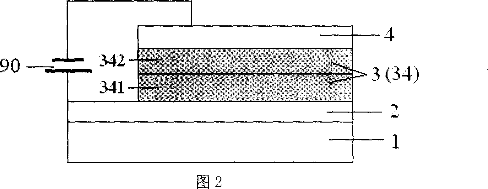
[0047] As shown in FIG. 5 , the organic functional layer 3 includes a hole injection layer 31 , a light emitting layer 34 , a hole blocking layer 35 , and an electron transport layer 36 , and the light emitting layer 34 includes a blue fluorescent light emitting layer 341 and a phosphorescent light emitting layer 342 . The hole injection layer 31 is made of CuPc. The material of the blue fluorescent emitting layer 341 is NPB. The phosphorescent light-emitting layer 342 emits yellow phosphorescence, and the material adopts (t-bt) 2 Ir(acac). The carrier material in the light emitting layer 34 is CBP. The material of the hole blocking layer 35 is BCP. The electron transport layer 36 material is Alq 3 . Transparent substrate 1 is made of glass. The material of the anode layer 2 is ITO. Cathode layer 4 is made of LiF thin layer and metal Al. The whole device structure can be described as:
[0048] Glass / ITO / CuPc / CBP:NPB / CBP:(t-bt) 2 Ir(acac) / BCP / Alq 3 / LiF / Al,
[0049]...
specific Embodiment approach 2
[0061] As shown in FIG. 6 , the organic functional layer 3 includes a hole injection layer 31 , a light emitting layer 34 , and an electron transport layer 36 , and the light emitting layer 34 includes a blue fluorescent light emitting layer 341 and a phosphorescent light emitting layer 342 . The hole injection layer 31 is made of CuPc. The material of the blue fluorescent emitting layer 341 is DPVBi. The phosphorescence emitting layer 342 emits red phosphorescence, and the material adopts (btp) 2 Ir(acac). The carrier material in the light emitting layer 34 is CDBP. The electron transport layer 36 material is Alq 3 . Transparent substrate 1 is made of glass. The material of the anode layer 2 is ITO. The cathode layer 4 is made of an alloy of Mg and Ag. The whole device structure can be described as:
[0062] Glass / ITO / CuPc / DPVBi / CDBP:(btp) 2 Ir(acac) / Alq 3 / Mg:Ag,
[0063] or
[0064] Glass / ITO / CuPc / CDBP:(btp) 2 Ir(acac) / CDBP:DPVBi / Alq 3 / Mg:Ag.
[0065] The fa...
specific Embodiment approach 3
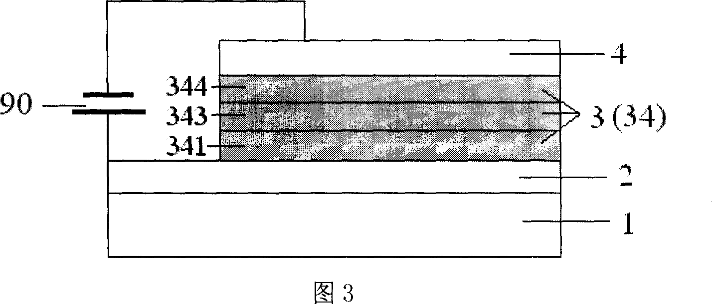
[0066] As shown in Figure 7, the organic functional layer 3 includes a hole injection layer 31, a light emitting layer 34, an electron transport layer 36 and a hole blocking layer 37, and the light emitting layer 34 includes a blue fluorescent light emitting layer 341, a red phosphorescent light emitting layer 343 and A green phosphorescence emitting layer 344 . The hole injection layer 31 is made of CuPc. The material of the blue fluorescent emitting layer 341 is NPB. Red phosphorescent light-emitting layer 343 material used (btp) 2 Ir(acac). The material of the green phosphorescence emitting layer 344 is Ir(ppy) 3 . The carrier material in the light emitting layer 34 is CBP. The material of the electron transport layer 36 is BCP. The hole blocking layer 37 is made of BCP. Transparent substrate 1 is made of glass. The material of the anode layer 2 is ITO. Cathode layer 4 is made of LiF thin layer and metal Al. The whole device structure can be described as:
[0067...
PUM
| Property | Measurement | Unit |
|---|---|---|
| Sheet resistance | aaaaa | aaaaa |
| Film thickness | aaaaa | aaaaa |
| Thickness | aaaaa | aaaaa |
Abstract
Description
Claims
Application Information