Driving chip packaging structure engaged by multilayer lug and driving chip

A technology for driving chips and bumps, which is applied to semiconductor/solid-state device components, semiconductor devices, electrical components, etc., and can solve problems that affect the strength of inner pins, inconvenience, and easy wear of probes

Inactive Publication Date: 2007-03-07
CHIPMOS TECH INC
View PDF0 Cites 6 Cited by
  • Summary
  • Abstract
  • Description
  • Claims
  • Application Information

AI Technical Summary

Problems solved by technology

[0003] A known bump structure is as disclosed in Taiwan Patent Announcement No. 488052 "Process of Forming Metal Bumps with More than Two Layers by Electroless Plating". Inner metal bumps, the material of the inner metal bumps is nickel, and its height is more than 15 μm, and a peripheral metal layer made of gold completely covers the outer periphery of the inner metal bumps, so that the double layer The total thickness of the above metal bumps is more than 18μm. After the bumps are formed on a plurality of solder pads of a chip, the wafer test step must be performed. During the wafer test process, the probes must be inserted into these solder pads. For the metal bumps with more than two layers on the pad, because the height of the peripheral metal layer (gold) is less than one-fifth of the inner layer metal bump (nickel), that is, the thickness of the gold layer is thinner, and the probe will be easily pierced. Penetrating the gold layer and touching the harder nickel layer makes the probe easy to wear. In severe cases, even the thickness of the gold

Method used


Image

  • Driving chip packaging structure engaged by multilayer lug and driving chip
  • Driving chip packaging structure engaged by multilayer lug and driving chip

Examples


Embodiment Construction

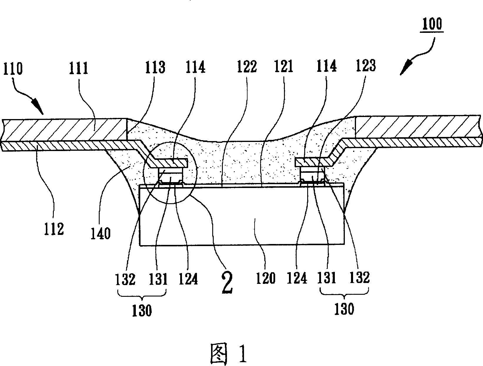
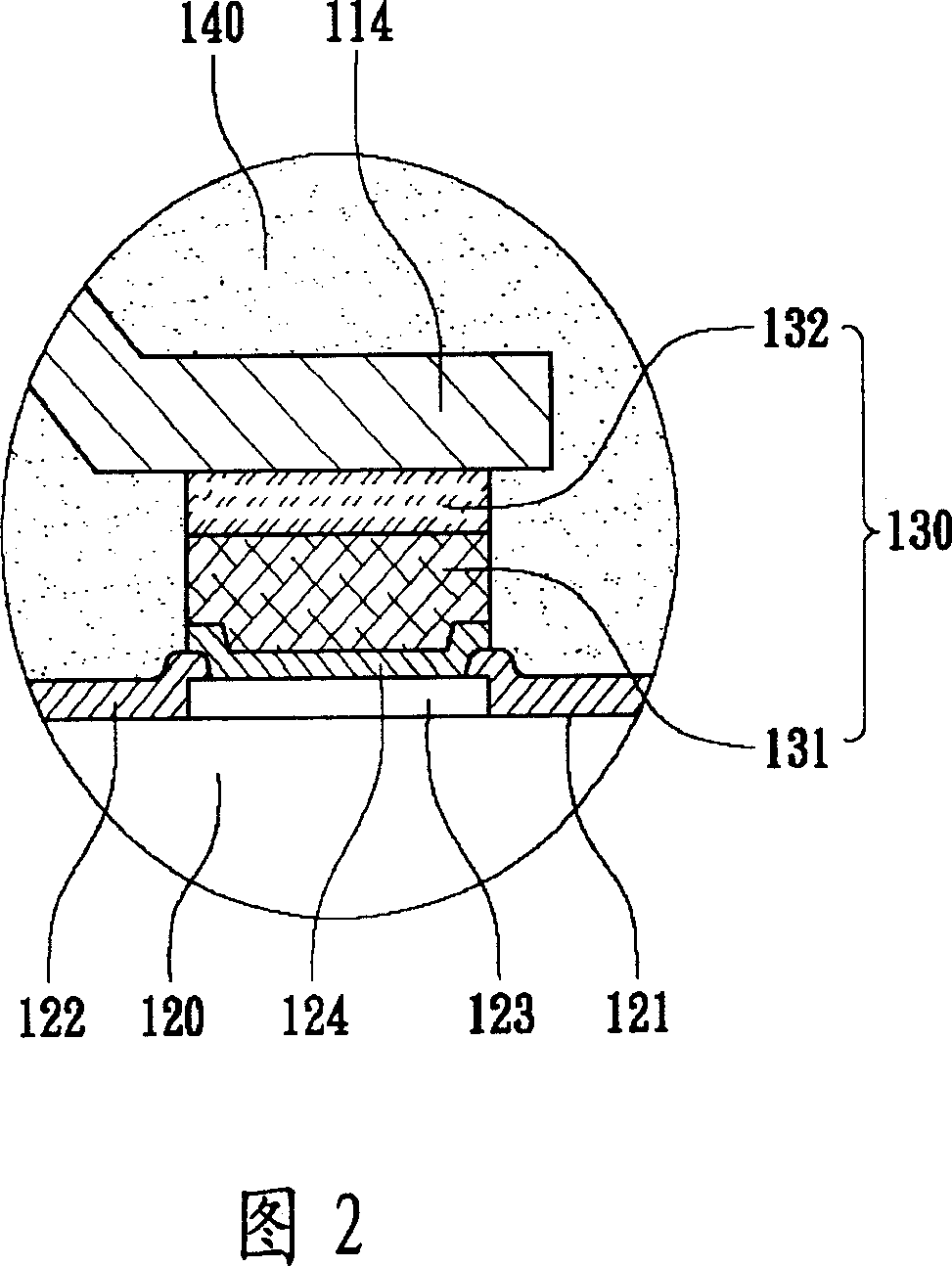
[0037] In order to further explain the technical means and effects of the present invention to achieve the intended purpose of the invention, in conjunction with the accompanying drawings and preferred embodiments, the driving chip packaging structure and the driving chip using multi-layer bump bonding proposed according to the present invention will be described below. Specific embodiments, structures, features and effects thereof are described in detail below.

[0038] Please refer to FIG. 1 and FIG. 2, which is a specific embodiment of the present invention. The driving chip package structure 100 utilizing multi-layer bump bonding includes a circuit film 110, and the circuit film 100 can be carried by a tape The tape (Tape) of packaging (TCP) or the film (Film) of chip-on-film packaging (COF) is exemplified by tape in this embodiment. The circuit film 110 includes an electrically insulating soft film body 111 and A conductive circuit layer 112, and the electrical insulation...


PUM


Abstract

This invention relates to drive chip seal structure and drive chip by use of multiple layer of protruding block, which comprises one circuit film and one drive chip, wherein, the film conductor circuit layer has multiple connection terminal; the drive chip has one active surface to form multiple weld pads and protruding blocks set on the main surface of chip to supply thermal binding bench connection terminals; each multiple protruding blocks comprise one basic metal layer and one binding metal layer.

Description

technical field [0001] The invention relates to a driving chip packaging structure, in particular to a driving chip packaging structure utilizing multi-layer bump bonding and a driving chip with multi-layer bumps. Background technique [0002] The conventional driver chip packaging structure includes Tape Carrier Package (TCP) or Chip On Film (COF), in which gold bumps are first formed on the pads of the driver chip, and then Thermal compression bonding to tape or film, and during the packaging process, because the hardness value of the gold bump changes too much, the process parameters must be controlled within a small range, that is, the process window (process window) ) is small, and the hardness value of the existing conventional gold bump is between Vickers hardness (Hv) 35 to 65, that is, the variation range is Vickers hardness 30, and the allowable inner lead bond (ILB) The parameter changes are small. [0003] A known bump structure is as disclosed in Taiwan Patent...

Claims


Application Information

Patent Timeline
IPC IPC(8): H01L23/48
CPCH01L2924/0002H01L24/50H01L2924/01322H01L2224/50H01L2924/00H01L2924/00012
Inventor 沈更新
Owner CHIPMOS TECH INC
Why Eureka
Try Eureka