
Semicoductor circuit, inverter circuit, semiconductor apparatus

A semiconductor and circuit technology, applied in semiconductor devices, semiconductor/solid-state device manufacturing, circuits, etc., can solve the problems of gas discharge current flow, cost increase, noise, etc., achieve simple circuit configuration, prevent noise, and low manufacturing cost Effect

Inactive Publication Date: 2007-03-21
FUJI ELECTRIC DEVICE TECH CO
View PDF2 Cites 6 Cited by
  • Summary
  • Abstract
  • Description
  • Claims
  • Application Information

AI Technical Summary

Problems solved by technology

Since a conventional driver circuit drives N at the same voltage as that at maximum load even at a light load as described above O 124 gate, thus causing a drastic output voltage change, and through N O The feedback capacitance of 124 causes noise which further causes overvoltage on VDD 123
However, the countermeasure described in Patent Document 1 cannot completely solve the above-mentioned problems
[0018] In the case where no next clock signal is input within a predetermined period of time after the last clock signal input, the method of reducing the gate voltage of the output device to prevent IC breakdown cannot allow sufficient gas discharge current to flow after the gas voltage is lowered
Therefore, the above-mentioned method results in a limitation on driving the plasma display panel
[0019] To eliminate the above problems, a more complex circuit configuration is proposed
However, it is difficult to adopt such a more complicated circuit configuration to a general circuit because a more complicated circuit configuration leads to an increase in cost and a detriment to higher circuit integration

Method used


Image

  • Semicoductor circuit, inverter circuit, semiconductor apparatus
  • Semicoductor circuit, inverter circuit, semiconductor apparatus
  • Semicoductor circuit, inverter circuit, semiconductor apparatus

Examples


Embodiment Construction

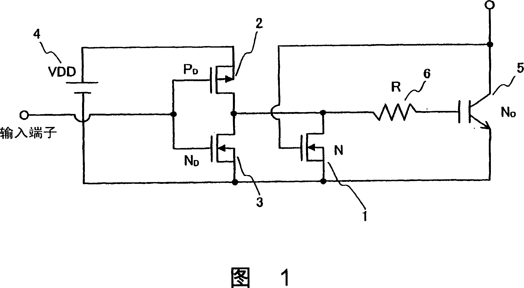
[0052] The invention will now be described in detail hereinafter with reference to the accompanying drawings, which show preferred embodiments of the invention.

[0053] A semiconductor circuit according to the present invention includes: an output semiconductor device; a driver circuit whose output terminal is connected to a control terminal of the output semiconductor device for driving the output semiconductor device; and a voltage-controlled semiconductor device which is controlled in response to the output potential of the output semiconductor device. Outputs the gate potential of a semiconductor device, or the power supply voltage of a driver circuit.

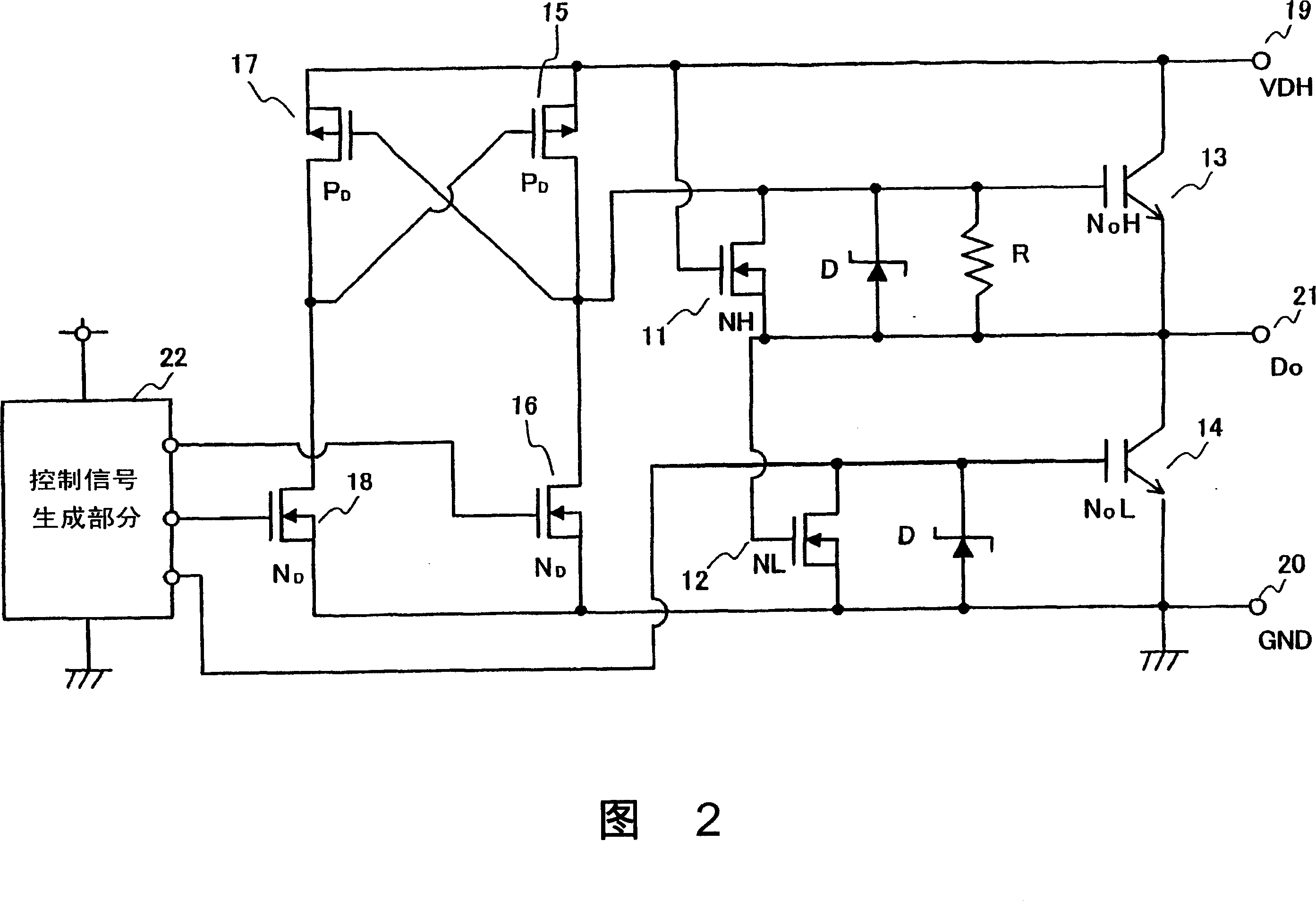
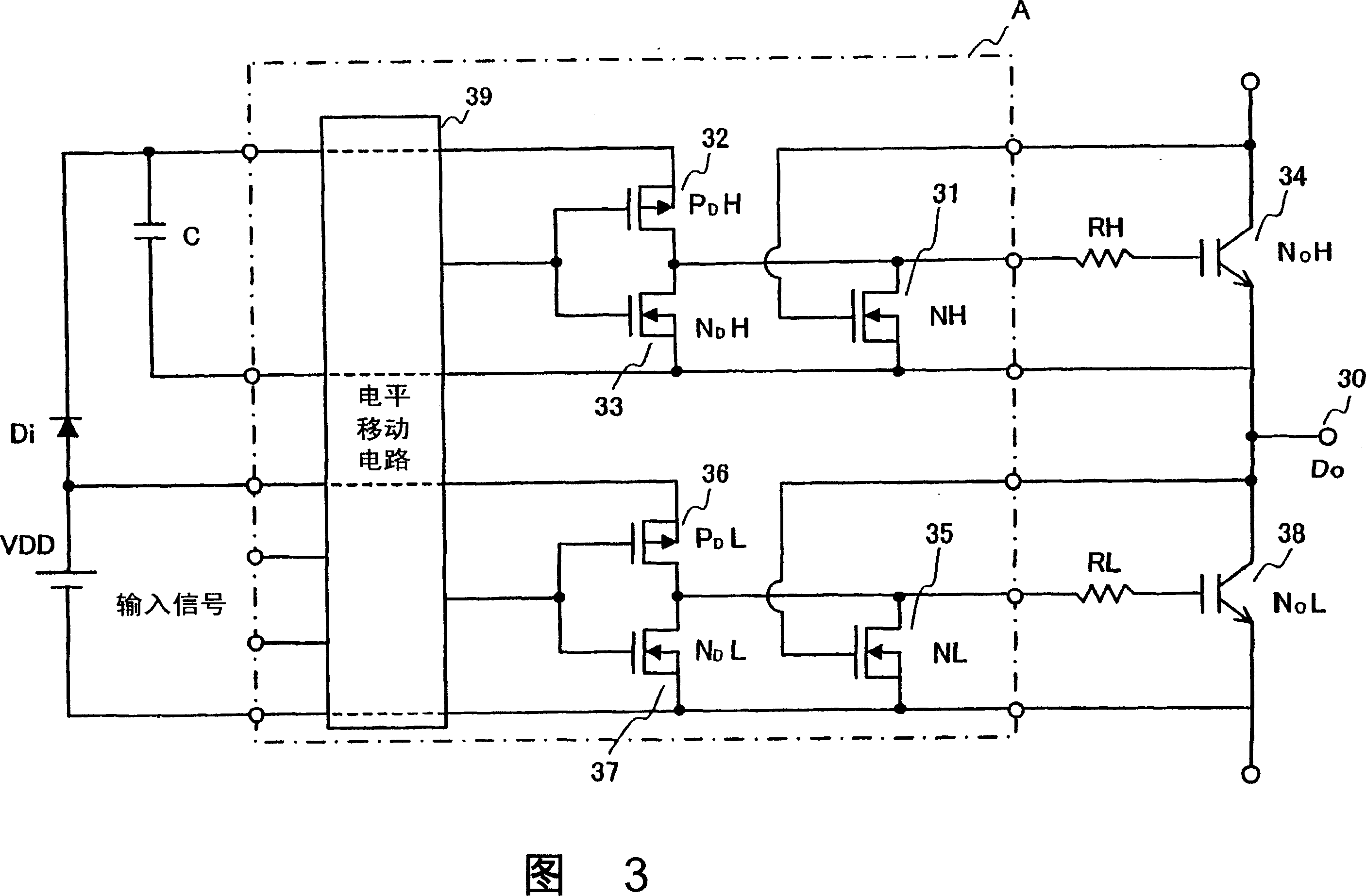
[0054] A circuit configuration according to a first embodiment of the present invention in which a voltage-controlled semiconductor device is used to control the gate potential of an output semiconductor device and a second embodiment according to the present invention in which a voltage-controlled semiconductor device is ...


PUM


Abstract

The semiconductor circuit includes a voltage-controlled semiconductor device (N)N, the resistance value of which is controllable with a high voltage, the drain terminal of the N can be connected to the gate terminal (control terminal) of an output semiconductor device (NO) via a resistor (R), the source terminal of the N is connected to the emitter terminal of the NO, and the gate terminal of the N is connected to the collector terminal, which is the output terminal, of the NO. When the input terminal of the semiconductor circuit is at the Hi-level, the NO OFF. By connecting the output terminal of the NO to the high-potential-side of a high-voltage circuit disposed separately and the negative electrode of a control power supply (VDD) to the low-potential-side of the high-voltage circuit in the state, a desired high voltage is applied between the collector and emitter of the NO. Since a p-channel MOSFET (PD) is turned ON as the input terminal potential is changed over to the Lo-level and the high voltage is still being applied to the output terminal of the NO, the N is turned ON and the NO is brought into the ON-state, in which the current driving ability of the NO is low. The semiconductor circuit can protect the devices from an over voltage with a simple circuit configuration.

Description

technical field [0001] The present invention relates to a semiconductor circuit, an inverter circuit, and a semiconductor device. More specifically, the present invention relates to a semiconductor circuit including a semiconductor device operating as an output device and a driver circuit whose output terminal is connected to a control terminal of the semiconductor device for driving the semiconductor device; an inverter circuit of a semiconductor circuit; and a semiconductor device including the semiconductor circuit or the inverter circuit as described above formed on a semiconductor substrate. Background technique [0002] Recently, a plasma display has been widely used as a next-generation display having a wide screen and replacing a Brownian tube. Mainly used alternating current (AC) plasma displays display images by causing gas discharge to occur by alternately feeding a discharge sustain pulse voltage to panel electrodes. [0003] A three-electrode surface discharge...

Claims


Application Information

Patent Timeline
Patent Type & Authority Applications(China)
IPC IPC(8): H01L27/02H03K19/20G09G3/288G09G3/20G09G3/296G09G3/298H01L21/822H01L27/04H03K17/08H03K17/56H03K17/687
CPCH01J2217/49G09G3/296
Inventor 岛袋浩小林英登重田善弘多田元
Owner FUJI ELECTRIC DEVICE TECH CO
Learn More