Bipolar electrostatic chuck

An electrostatic chuck, bipolar technology, applied to the application of electrostatic attraction holding device, circuit, electrical components, etc., can solve the problems that it is difficult to remove the sample, cannot exert sufficient adsorption force, etc.

Inactive Publication Date: 2007-03-21
CREATIVE TECH CORP
View PDF3 Cites 6 Cited by
  • Summary
  • Abstract
  • Description
  • Claims
  • Application Information

AI Technical Summary

Problems solved by technology

Therefore, in the aforementioned bipolar electrostatic chuck that narrows the original electrode spacing, the actual voltage that can be applied is limited. Compared with glass substrates used in flat panel displays, there is a problem that sufficient adsorption force (gradient force) cannot be exerted due to the increase in weight per unit area
[0012] On the other hand, when an insulating sample is adsorbed by an electrostatic chuck, even if the voltage applied to the electrode is cut off, there is a problem that it is difficult to remove the sample from the sample adsorption surface of the electrostatic chuck due to

Method used


Image

  • Bipolar electrostatic chuck
  • Bipolar electrostatic chuck
  • Bipolar electrostatic chuck

Examples


Embodiment 1

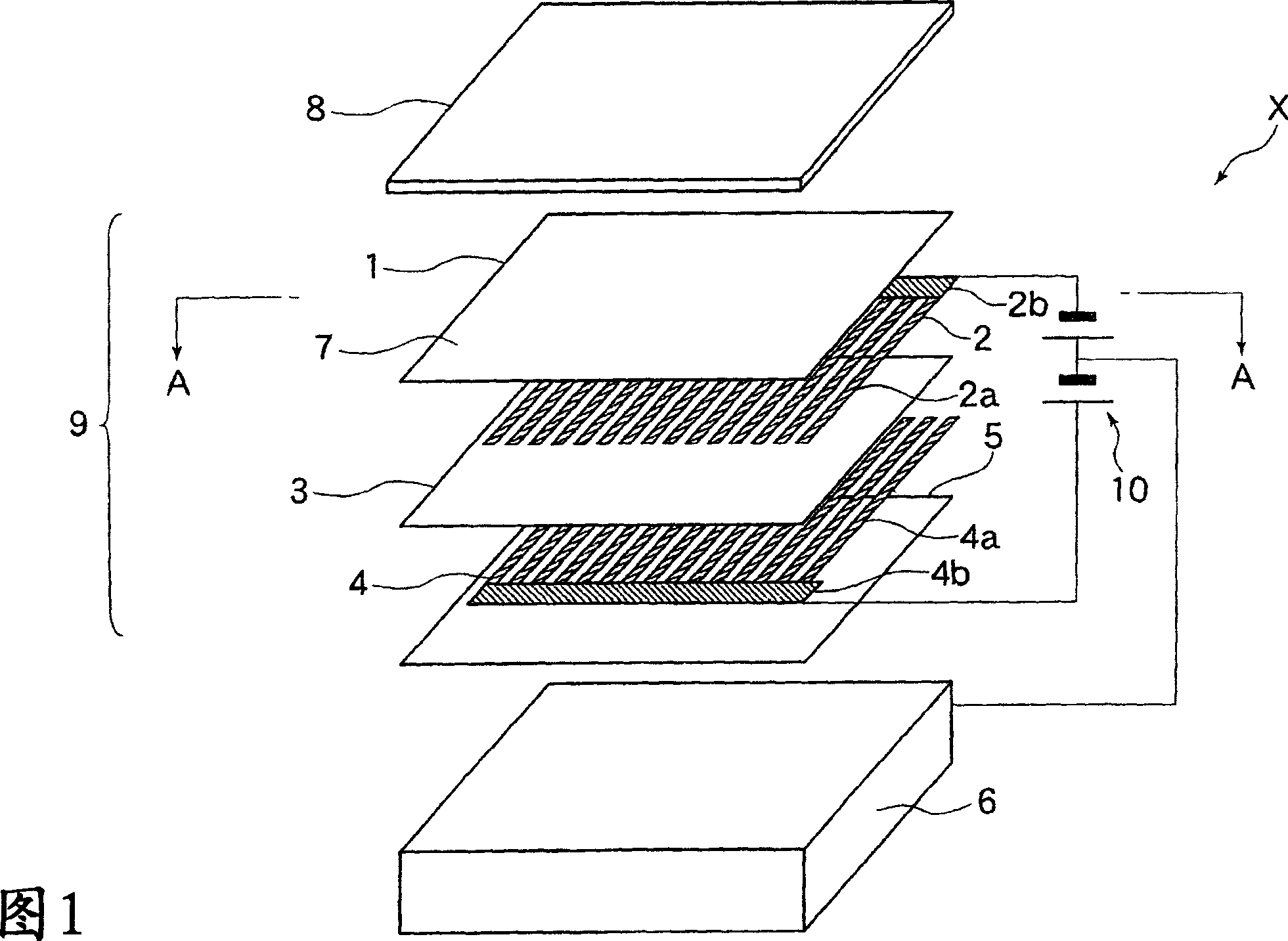
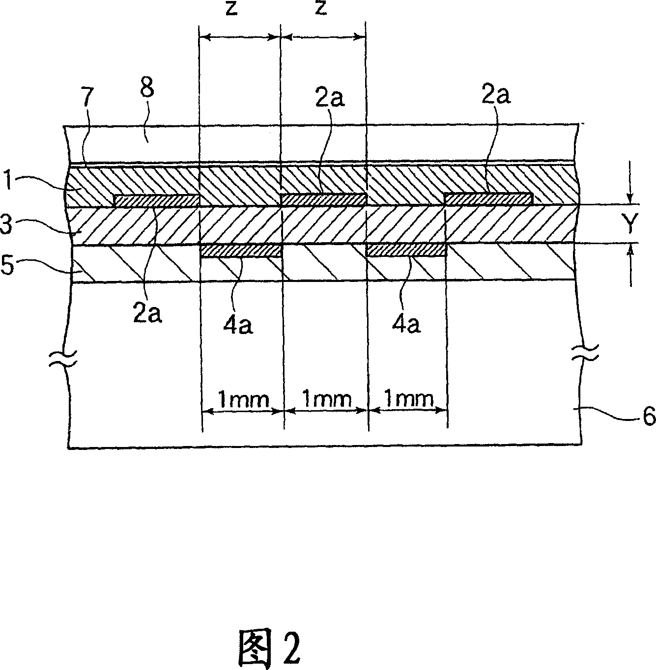
[0098] Fig. 1 shows the disassembled oblique view explanatory diagram of the bipolar electrostatic chuck of embodiment 1, this bipolar electrostatic chuck X comprises: length 100mm * width 100mm, film thickness 50μm and resistivity ε=3.5, has thermoplastic polymer on the lower surface An upper insulating layer 1 composed of a polyimide film of an imide film; a first electrode 2 composed of copper with a film thickness of 3 μm; a polyimide film with a length of 100 mm×width of 100 mm, a film thickness of 50 μm, and a resistivity ε=3.5 The inter-electrode insulating layer 3 composed; the second electrode 4 composed of copper with a film thickness of 3 μm; length 100 mm×width 100 mm, film thickness 50 μm and resistivity ε=3.5, polyimide with thermoplastic polyimide on the upper surface The lower insulating layer 5 is made of amine film; the metal substrate 6 is composed of aluminum with a length of 100 mm x a width of 100 mm x a thickness of 10 mm. In addition, in this bipolar el...

Embodiment 2

[0106] 4 is a cross-sectional explanatory diagram of the bipolar electrostatic chuck X of Example 2, and FIG. 5 is the normal line of the first electrode 1 and the second electrode 14 of the bipolar electrostatic chuck X of Example 2 along the sample adsorption surface 7. Partial plane explanatory diagram when viewed from the direction.

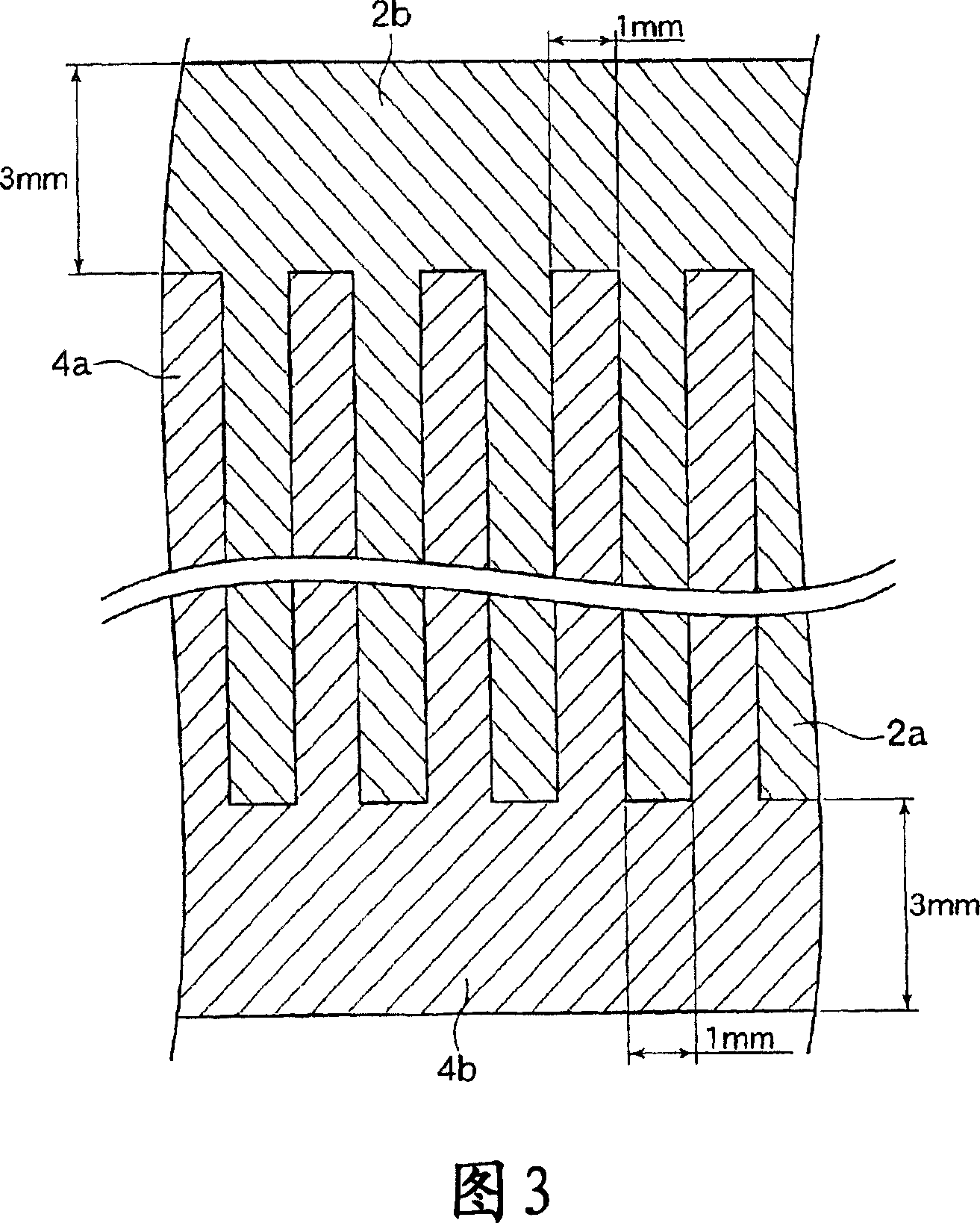
[0107] In the bipolar electrostatic chuck X of Embodiment 2, the electrode width of the strip-shaped portion 14a of the second electrode 14 is formed at 0.6 mm, and the strip-shaped portion 14a of the second electrode 14 is located on the strip-shaped portion formed by the first electrode 2. In the center of the gap (1 mm) formed by 2a, the strip-shaped comb teeth of the first electrode 2 and the strip-shaped comb teeth of the second electrode 14 are combined alternately, and the first electrode 2 and the strip-shaped comb teeth of the second electrode 14 are combined along the normal direction of the sample adsorption surface 7. The second e...

Embodiment 3

[0109] Fig. 6 is an exploded oblique view explanatory diagram of the bipolar electrostatic chuck X of embodiment 3, Fig. 7 is an explanatory diagram of a section (a part of section A-A in Fig. 6 ) of the bipolar electrostatic chuck X of embodiment 3, and Fig. 8 is an explanatory diagram of the embodiment 3 is a partial plan view of the first electrode 2 and the second electrode 24 of the bipolar electrostatic chuck X viewed along the normal direction of the sample adsorption surface 7 . The dotted area in FIG. 8 represents the portion where the second electrode 24 overlaps the first electrode 2 along the normal direction of the sample adsorption surface 7 .

[0110] The bipolar electrostatic chuck X of Example 3 was completed under the same conditions as in Example 1, except that the second electrode 24 was formed into a flat plate having a planar area of ​​80 mm in length and 80 mm in width.


PUM

PropertyMeasurementUnit
Thicknessaaaaaaaaaa
Radiusaaaaaaaaaa

Abstract

A bipolar electrostatic chuck which has excellent dielectric breakdown strength and provides excellent attracting performance. The bipolar electrostatic chuck eliminates difficulty in peeling off a sample from a sample attracting plane as much as possible after application of a voltage to electrodes is finished. The bipolar electrostatic chuck is provided with a first electrode and a second electrode in an insulator and permits a surface of the insulator to be the sample attracting plane. The insulator has the first electrode, an interelectrode insulating layer and the second electrode in this order from the sample attracting plane in the depth direction. The second electrode has a region not overlapping with the first electrode in a normal line direction of the sample attracting plane.

Description

technical field [0001] The present invention relates to a bipolar electrostatic chuck for holding a sample by electrostatic adsorption. Background technique [0002] Etching equipment, plasma processing equipment for forming thin films by chemical vapor deposition (CVD), electron exposure equipment, ion writing equipment, ion implantation equipment, etc., used for semiconductor manufacturing processes required to form integrated circuits on semiconductor wafers such as silicon It is widely used in the manufacturing process of liquid crystal display panels used in the manufacturing process of liquid crystal display panels used in television screens and computer monitors, etc. An electrostatic chuck is used to hold samples such as wafers and glass by electrostatic attraction. Compared with the method of holding by mechanical devices, the electrostatic chuck can play its role in the damage of the sample, the yield problem caused by the broken particles caused by mechanical con...

Claims


Application Information

Patent Timeline
IPC IPC(8): H01L21/68H02N13/00
Inventor 藤泽博宫下欣也
Owner CREATIVE TECH CORP
Why Eureka
Try Eureka