Cobalt silicon contact barrier metal process for high density semiconductor power devices

An oxide semiconductor and metal technology, applied in semiconductor devices, semiconductor/solid-state device manufacturing, electric solid-state devices, etc., can solve problems such as loss of dopants at the contact interface

Active Publication Date: 2007-04-04
ALPHA & OMEGA SEMICON CAYMAN
View PDF1 Cites 6 Cited by
  • Summary
  • Abstract
  • Description
  • Claims
  • Application Information

AI Technical Summary

Problems solved by technology

[0007] Therefore, the object of the present invention is to provide a new and improved semiconductor power device using cobalt-silicon metal insulating contacts, so as to solve the problem of contact interface dopant loss, thereby overcoming the limitations of traditional methods

Method used


Image

  • Cobalt silicon contact barrier metal process for high density semiconductor power devices
  • Cobalt silicon contact barrier metal process for high density semiconductor power devices
  • Cobalt silicon contact barrier metal process for high density semiconductor power devices

Examples


Embodiment Construction

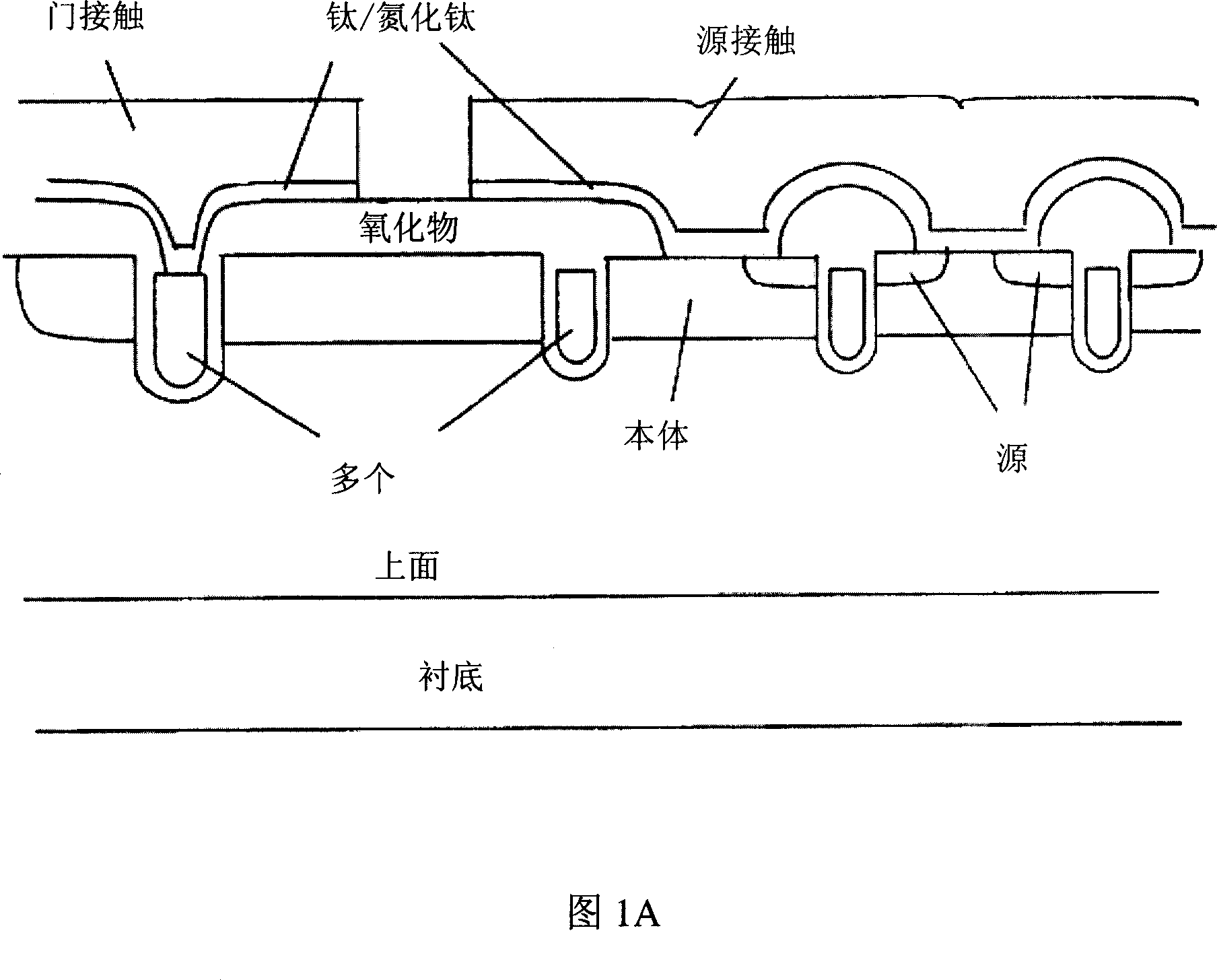
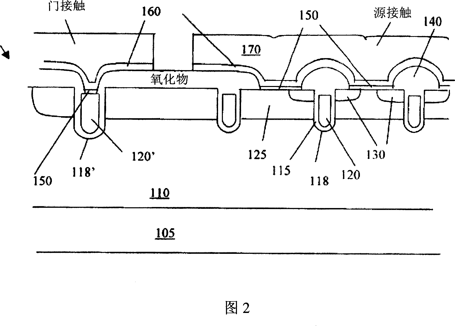
[0015] Turn now to the cross-sectional view of trench DMOS device 100 in FIG. 2 . The trench DMOS device 100 is supported on a substrate 105 including an epitaxial layer 110 and includes a trench gate 120 in a trench 118 with a gate insulating layer 115 formed over the trench walls. The body region 125 doped with a second conductivity type, such as a P-type dopant, extends between the trench gates 120, and the P-body region 125 surrounding the source region 130 adopts the first conductivity type, such as N+ doping agent doping. The active region 130 is formed around the top surface of the epitaxial layer surrounding the trench gate 120 , and the top surface of the semiconductor substrate extending to the top of the trench gate, P-body region 125 and source region 130 is covered with a dielectric capping layer 140 . Trench DMOS device 100 also includes an insulating gate runner 120' arranged in gate runner trench 118', and connected to gate 120, the connections of which are no...


PUM


Abstract

The invention provides an improved trenched metal oxide semiconductor field effect transistor (MOSFET) cell that includes a trenched gate surrounded by a source region encompassed in a body region above a drain region disposed on a bottom surface of a substrate. The MOSFET cell further includes a source contact opening opened on top of an area extended over the body region and the source region through a protective insulation layer, wherein the area further has a cobalt-silicide layer disposed near a top surface of the substrate. The MOSFET cell further includes a Ti / TiN conductive layer covering the area interfacing with the cobalt-silicide layer over the source contact opening. The MOSFET cell further includes a source contact metal layer formed on top of the Ti / TiN conductive layer ready to form source-bonding wires thereon.

Description

technical field [0001] The present invention generally relates to semiconductor power devices, and in particular to an improved and new contact insulating metal process, which can produce high-density semiconductor power devices with improved source contact resistance by improving the source contact interface layer structure. Background technique [0002] Since the advent of high-efficiency metal-oxide-semiconductor (MOS) gate devices in portable electronic devices, power conversion applications have required more stringent further reductions in the turn-on resistance of metal-oxide-semiconductor field-effect transistor (MOSFET) devices. To meet this requirement, larger diameter wires have been bonded together to improve the connection of the semiconductor die to the external leads. When using combined larger diameter wires, the traditional process of producing trench MOSFETs with either no metal insulation or titanium / titanium nitride (Ti / TiN) insulation when in contact wit...

Claims


Application Information

Patent Timeline
Patent Type & Authority Applications(China)
IPC IPC(8): H01L29/78H01L27/02H01L21/336H01L21/82
CPCH01L21/76843H01L21/28518H01L29/66734H01L29/4941H01L29/4933H01L29/456H01L29/7811H01L21/76855H01L29/7813
Inventor 常虹李铁生戴嵩山伍明谦安荷叭剌
Owner ALPHA & OMEGA SEMICON CAYMAN
Why Eureka
Try Eureka