Semiconductor device and method of manufacturing such a device

A technology of semiconductors and devices, applied in the field of semiconductor devices, capable of solving problems such as effective resistance reduction

Active Publication Date: 2012-09-26
NXP BV
View PDF1 Cites 0 Cited by
  • Summary
  • Abstract
  • Description
  • Claims
  • Application Information

AI Technical Summary

Problems solved by technology

[0006] A disadvantage of this known device is that sometimes it still exhibits problems corresponding to a reduction in the effective resistance of the high-ohmic semiconductor substrate

Method used


Image

  • Semiconductor device and method of manufacturing such a device
  • Semiconductor device and method of manufacturing such a device
  • Semiconductor device and method of manufacturing such a device

Examples


Embodiment Construction

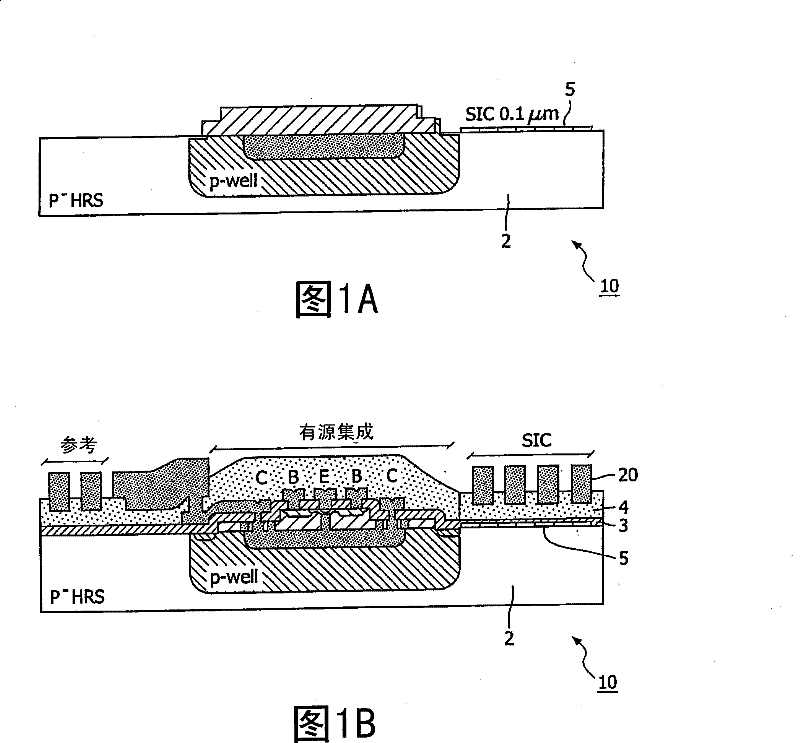
[0053] Figure 1A -B is a schematic cross-sectional view perpendicular to the thickness direction of the semiconductor device according to the present invention. The semiconductor device 10 comprises a semiconductor body 1 with a p-type silicon semiconductor substrate 2 which, in the present embodiment, has a resistivity of 2-4 KΩcm.

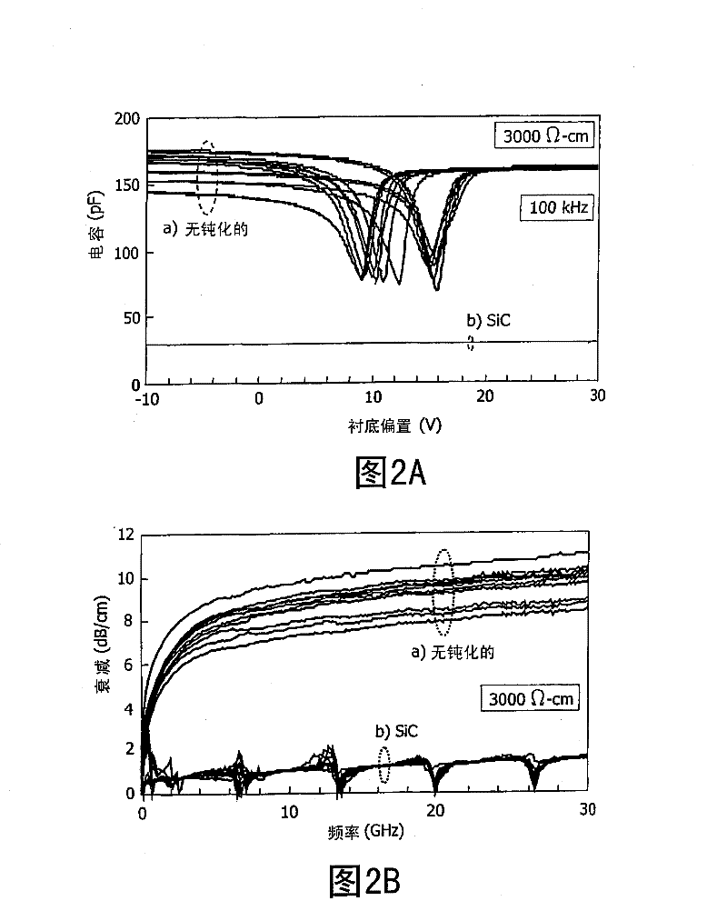
[0054] A 100-nm low-stress PECVD SiC film was disposed on a p-type high-resistivity substrate (HRS). The SiC film provides HRS surface passivation before the device integration process flow, ie equivalent to the original wafer in standard silicon processes.

[0055] A Novellus Concept One PECVD system was used to deposit amorphous SiC films. The main deposition parameters used for SiC deposition are: SiH at 400 °C, 2.25 Torr, and 100 sccm gas flow 4 and 3000sccm CH 4 , and a power of 1000W (HF=500W; LF=500W). The deposition rate of SiC using the above deposition parameters was 670 Angstroms / minute with a uniformity of about 1%. A refractive...


PUM


Abstract

The invention relates to a semiconductor device (10) comprising a semiconductor body (1) with a high-ohmic semiconductor substrate (2) which is covered with a dielectric layer (3, 4) containing charges, on which dielectric layer one or more passive electronic components (20) comprising conductor tracks (20) are provided, wherein, at the location of the passive elements (20), a region (5) is present at the interface between the semiconductor substrate (2) and the dielectric layer (3, 4), as a result of which the conductivity of an electrically conducting channel induced in the device (10) by the charges is limited at the location of the region (5). According to the invention, the region (5) is formed by deposition and comprises a semi-insulating material. As a result, the device (10) has avery low high-frequency power loss because the inversion channel is formed in the semi-insulating region (5). The device (10) further allows for a higher temperature budget and hence for the integration of active semiconductor elements (8) into the semiconductor body (1). A very suitable semi-insulating material for the region (5) is SiC, SIPOS or POLYDOX.

Description

technical field [0001] The invention relates to a semiconductor device comprising a semiconductor body having a high-ohmic semiconductor substrate covered with a charge-containing dielectric layer on which one or more passive devices comprising conductor tracks are arranged. Electronic components in which, at the location of the passive components, there is a region at the interface between the semiconductor substrate and the dielectric layer such that the conductivity of the conduction channel induced by electric charges in the semiconductor device is at the location of the region decrease. Background technique [0002] In this application, "high-ohmic semiconductor substrate" means in particular a semiconductor substrate whose resistivity is greater than or equal to about 1 kΩcm, indeed in the range between 1 and 10 kΩcm. [0003] High-resistivity silicon (HRS) has long been considered a potential Ideal substrate for integrating radio frequency (RF) circuits. However, t...

Claims


Application Information

Patent Timeline
Patent Type & Authority Patents(China)
IPC IPC(8): H01L27/08H01L27/06
CPCH01L27/08H01L27/0641H01L27/06
Inventor 维布·D.·范诺尔特彼德鲁斯·H.·C.·马格内利斯·K.·南维尔塞利内·J.·德切维尔里拉蒙·J.·黑文斯
Owner NXP BV
Why Eureka
Try Eureka