Masked cation exchange lithography

a technology of colloidal nanocrystals and lithography, which is applied in the field of colloidal nanocrystals film patterning, can solve the problems of not providing the possibility of interfacing nanoparticles with different compositions using a single lithography step, not providing nanoscale resolution, and not allowing to deposit “pure” nc films, etc., and achieves new versatility and high resolution

Active Publication Date: 2018-12-25
FOND INST ITAL DI TECH
View PDF8 Cites 0 Cited by
  • Summary
  • Abstract
  • Description
  • Claims
  • Application Information

AI Technical Summary

Benefits of technology

[0016]The present invention offers many advantages. It allows to chemically transform selected regions of arbitrary shapes in an otherwise homogeneous NC film. The masked cation exchange process is suitable to fabricate luminescent patterns and electrical circuits in NC films without altering their morphology, adding new versatility to these materials. Other advances in this direction are brought about by the high resolution that can be achieved in designing patterns. The claimed method also enables performing several cation exchange steps and therefore the assembly of several different materials in a single film. Finally, the masked cation exchange technique has the potential to integrate miniaturized opto-electronic elements, for example on well-defined areas on a microchip, offering a possible new technology for future integrated circuits.

Problems solved by technology

This method is resist free, can achieve arbitrary patterns with some tens of nm resolution, but as above, it does not provide the possibility to interface nanoparticles with different compositions using a single lithography step, as in the method of the present invention, and it does not result in a layer with homogeneous morphology (John Thomas P. et al.
This method does not allow to deposit “pure” NC films, does not provide nanoscale resolution and the pattern consists of filled and empty spaces.
This method relies also on the modification of the surface ligands by electron-beam exposure, but again produces patterns that consists of filled an empty spaces, and is not able to produce different materials in the same layer (Bedson T. R. et al.

Method used


Image

  • Masked cation exchange lithography
  • Masked cation exchange lithography
  • Masked cation exchange lithography

Examples


example 1

Nanocrystal Synthesis

[0054]CdSe nanocrystals (protocol as published by Talapin D. V. et al. Chem. Rev. 2010, 110(1): 389-458): TOPO (3.0 g), ODPA (0.280 g) and CdO (0.060 g) were mixed in a 50 ml flask, heated to ca. 150° C. and exposed to vacuum for ca. 1 hour. Then, under nitrogen, the solution was heated to 370° C. to dissolve the CdO until it turned optically clear and colorless. At this point, 1.5 g of TOP was injected in the flask and the temperature was allowed to recover, followed by the injection of the Se:TOP solution (0.058 g Se+0.360 g TOP).

[0055]After the synthesis, the nanocrystals were washed by addition of methanol, precipitated, and redispersed in toluene.

[0056]CdS nanorods: 50 mg of Cadmium oxide (CdO), 10 mg of cadmium chloride (CdCl2), 280 mg of octadecylphosphoric acid (ODPA), 80 mg of hexcylphosphonic acid (HPA), and 3 g of trioctylphosphine oxide (TOPO) were loaded in a reaction flask and then heated to 120° C. under vacuum for 1 h. Nitrogen was then pumped in...

example 2

Preparation of the NC Film and Cation Exchange

2.1. Deposition on Solid Substrate

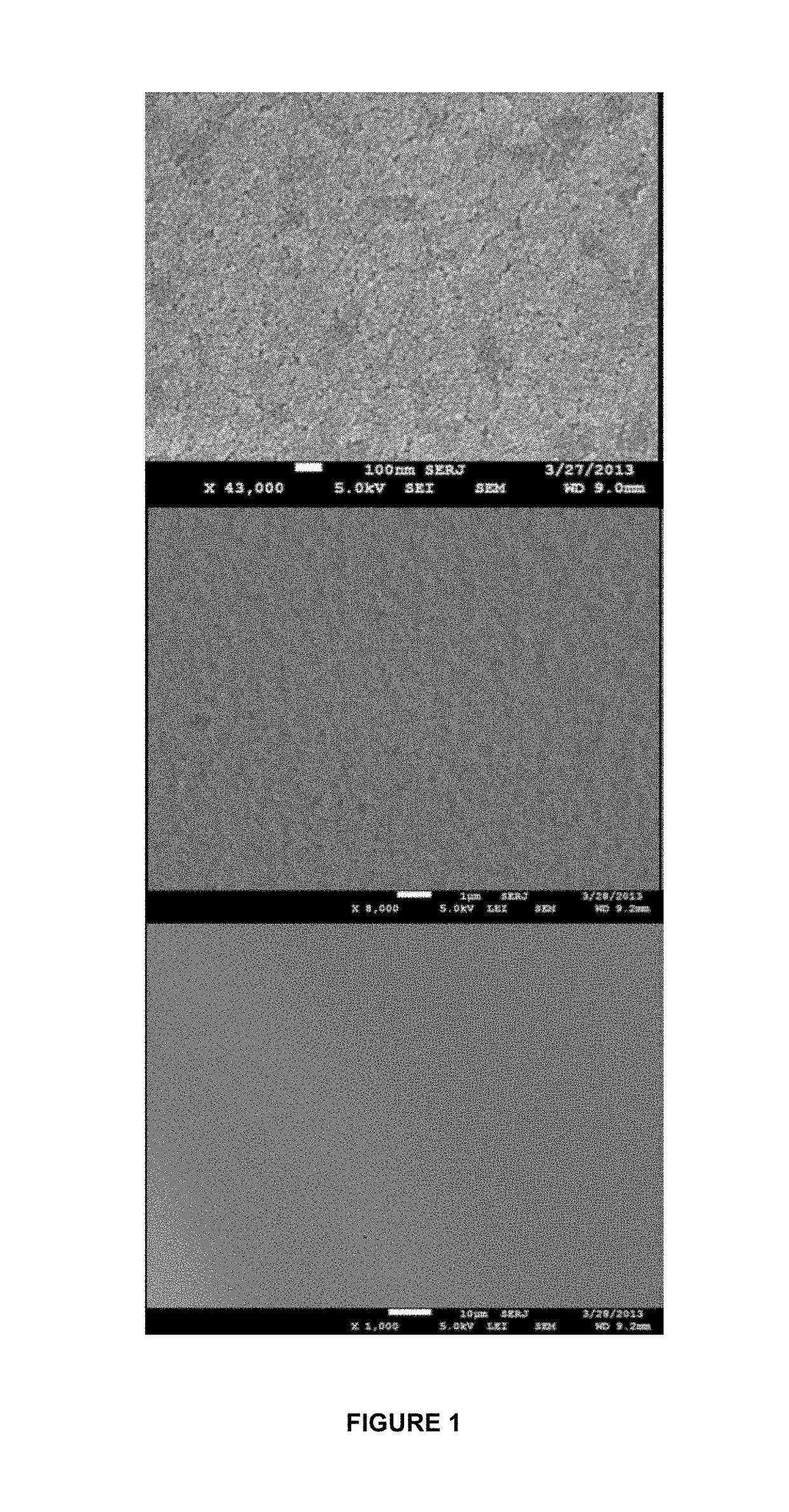
[0059]Homogeneous NC films were deposited on a substrate, for example, by spin coating or via layer-by-layer deposition. The NC films with thickness of few monolayers, were spin-coated from a toluene solution onto Si / SiO2 substrates. In detail, 15 μL of NC solution at a concentration of 2 μM was deposited on previously cleaned Si / SiO2 substrates, already mounted in the spin coater, and after 2 min the sample was spun at 2500 rpm for 4 min. The uniformity of the obtained NC films even over large areas is clearly seen in FIG. 1.

2.2. Irradiation

[0060]In the next step, the NC films were exposed to an electron-beam using a Raith 150-two lithography system, with an acceleration voltage of 10 kV and an exposure dose in the range of 0.1-20 mC / cm2.

2.3. Cation Exchange

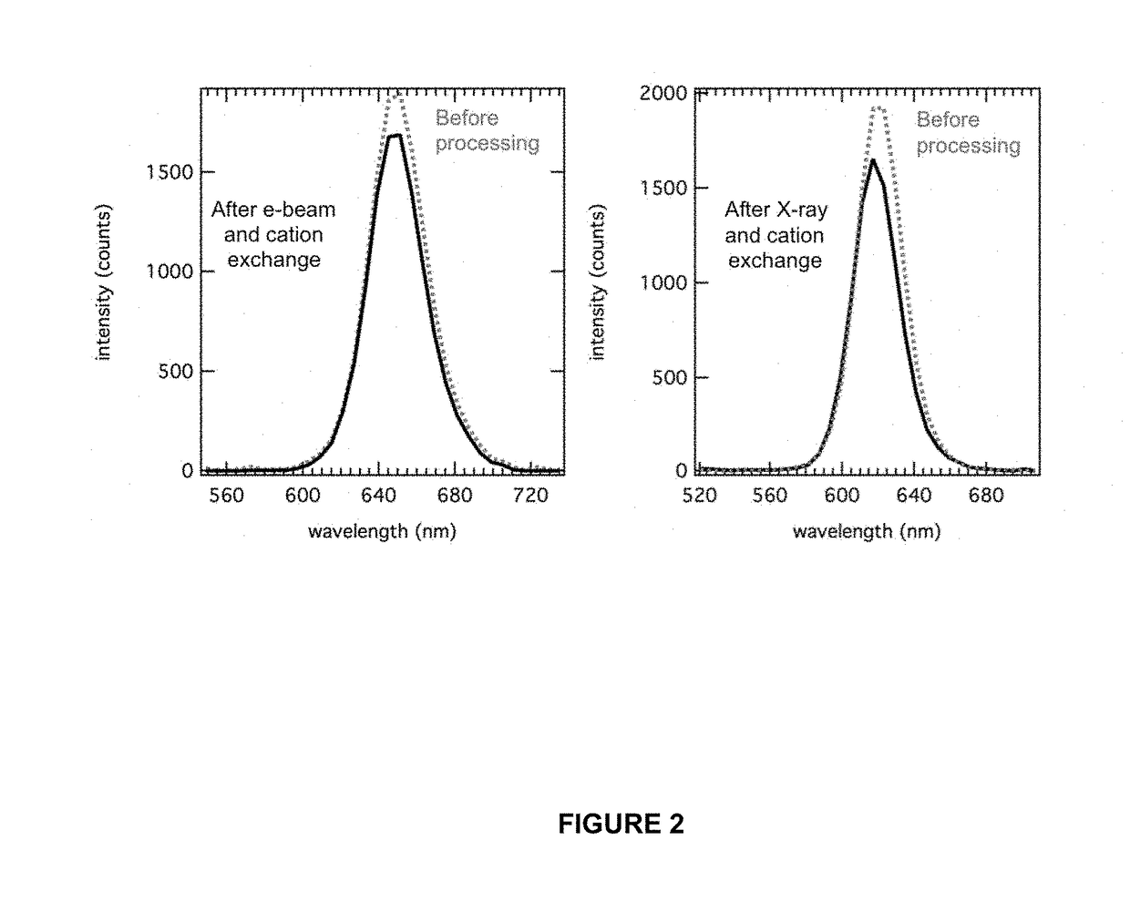
[0061]In this example, CdSe / CdS NCs were converted to Cu2-xSe / Cu2-xS following published cation exchange procedures (Jain P. K. et al. J. Am. Chem. ...

example 3

Masked Cation Exchange in CdSe Nanocrystal Films

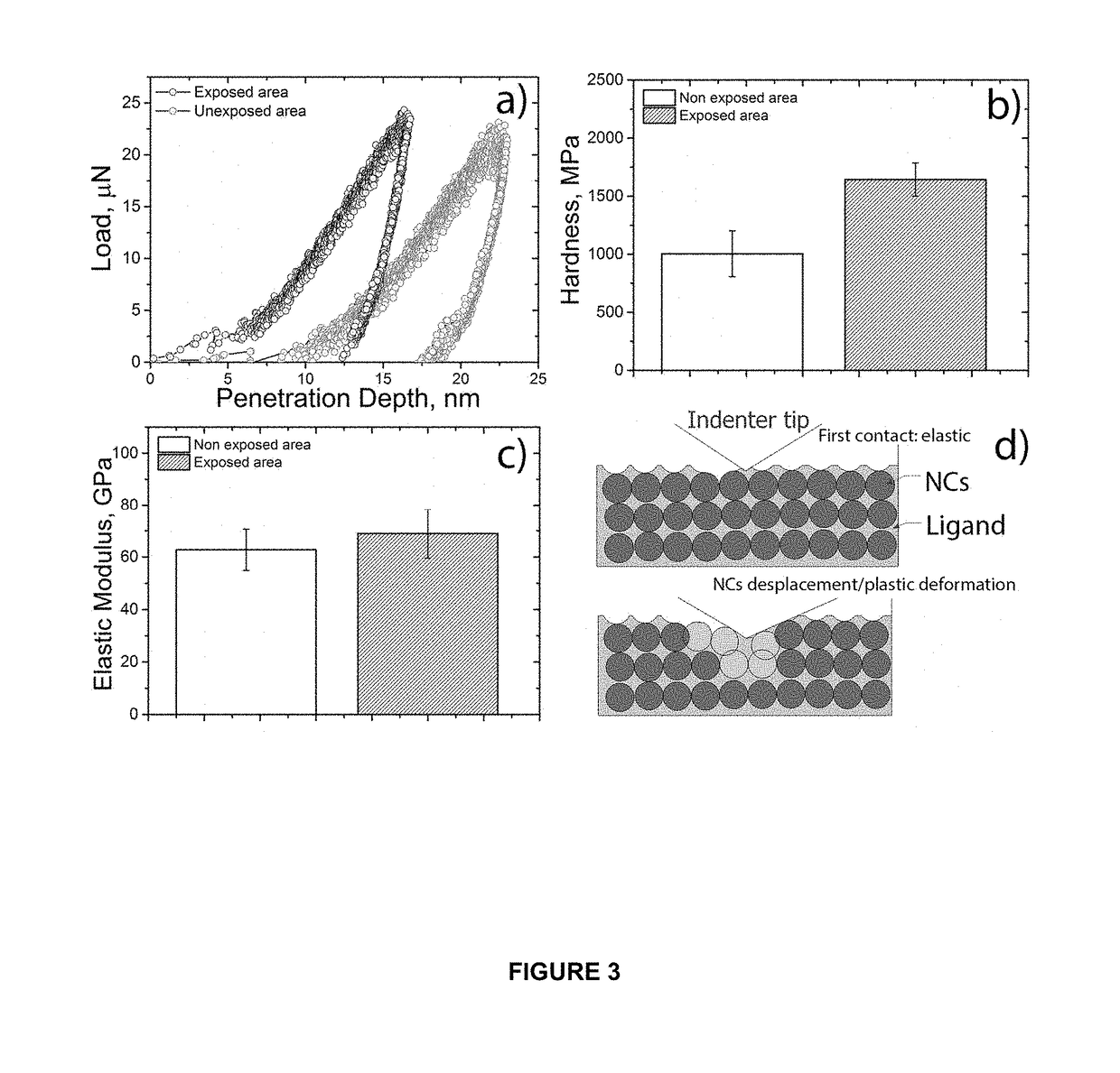
[0070]The “masked cation exchange” approach according to the present application, applied to Cd chalcogenide films, can be used to create luminescent patterns in NC films, and to fabricate electrical circuit patterns. FIG. 7a shows a Photo Luminescence (PL) image of a NC film where two pads are connected by a straight wire with 10 μm width: here pads and wire consist of Cu2-xSe / Cu2-xS, whereas the surrounding material is CdSe / CdS. For these experiments, the samples were kept under air for 24 h prior to measurements. Electrical measurements under ambient conditions were performed with a micromanipulator probe station (Suss) using tungsten micromanipulators as probes. The current was recorded with a Keithley 2612 source-meter. The current measured on the wire connecting the two pads is reported in FIG. 7b by the solid black line, yielding Ohmic conductivity of 250 μS / cm, while the CdSe / CdS regions did not conduct any current above the de...


PUM

PropertyMeasurementUnit
thicknessaaaaaaaaaa
temperaturesaaaaaaaaaa
temperatureaaaaaaaaaa

Abstract

We describe a method for patterning of colloidal nanocrystals films that combines a high energy beam treatment with a step of cation exchange. The high energy irradiation causes cross-linking of the ligand molecules present at the nanocrystal surface, and the cross-linked molecules act as a mask for the subsequent cation exchange reaction. Consequently, in the following step of cation exchange, the regions that have not been exposed to beam irradiation are chemically transformed, while the exposed ones remain unchanged. This selective protection allows the design of patterns that are formed by chemically different nanocrystals, yet in a homogeneous nanocrystal film.

Description

FIELD OF THE INVENTION[0001]The present invention relates to a method for patterning of colloidal nanocrystals films that combines a high energy beam treatment with a step of cation exchange. The high energy irradiation causes cross-linking of the ligand molecules present at the nanocrystal surface, and the cross-linked molecules act as a mask for the subsequent cation exchange reaction. Consequently, in the following step of cation exchange, the regions that have not been exposed to beam irradiation are chemically transformed, while the exposed ones remain unchanged. This selective protection allows the design of patterns that are formed by chemically different nanocrystals, yet in a homogeneous nanocrystal film.STATE OF THE ART[0002]Colloidal inorganic nanocrystals (NCs) are among the most exploited nanomaterials due to their extreme versatility. They are synthesized directly in the liquid phase and couple the advantage of being made of a core of one or more inorganic materials, w...

Claims


Application Information

Patent Timeline
Patent Type & Authority Patents(United States)
IPC IPC(8): C09K11/88G03F7/038G03F7/004B82Y40/00G03F7/26
CPCC09K11/881B82Y40/00G03F7/265G03F7/0047G03F7/038C09K11/88
Inventor KRAHNE, ROMANMISZTA, KAROLTOMA, ANDREAGREULLET, FANNYMARRAS, SERGIOPRATO, MIRKOARCINIEGAS, MILENAMANNA, LIBERATO
Owner FOND INST ITAL DI TECH
Why Eureka
Try Eureka