OLED packaging method and OLED package structure

a technology of oled packaging and oled structure, which is applied in the field of display technology, can solve the problems of reducing the brightness and reducing density, transmission rate, refractive index, etc., and achieves the effect of prolonging the service life of oled devices and high light output efficiency of oled devices

Active Publication Date: 2019-04-02
WUHAN CHINA STAR OPTOELECTRONICS TECH CO LTD
View PDF6 Cites 0 Cited by
  • Summary
  • Abstract
  • Description
  • Claims
  • Application Information

AI Technical Summary

Benefits of technology

[0009]Objectives of the present invention are to provide an OLED packaging method, which greatly extends the service life of an OLED device and also ensures a relatively high light output efficiency of the OLED device.
[0010]Objectives of the present invention are also to provide an OLED package structure, which greatly extends the service life of an OLED device and also ensures a relatively high light output efficiency of the OLED device.
[0034]The efficacy of the present invention is that the present invention provides an OLED packaging method and an OLED package structure. The OLED packaging method of the present invention is such that a silicon-doped diamond-like carbon layer and a diamond-like carbon scattering layer are both provided in an OLED package structure so that the silicon-doped diamond-like carbon layer may provide an effect of blocking external moisture and oxygen and the diamond-like carbon scattering layer is used to provide an effect of increasing light transmission rate, whereby it is possible to greatly extend the service life of the OLED device and also to ensure a relatively high light output efficiency of the OLED device. The OLED package structure of the present invention is such that a silicon-doped diamond-like carbon layer and a diamond-like carbon scattering layer are both provided, so that the silicon-doped diamond-like carbon layer may provide an effect of blocking external moisture and oxygen and the diamond-like carbon scattering layer is used to provide an effect of increasing light transmission rate, whereby it is possible to greatly extend the service life of the OLED device and also to ensure a relatively high light output efficiency of the OLED device.

Problems solved by technology

The OLED device is very sensitive to moisture and once exposed in moisture, the cathode might get oxidized and the organic layers (the hole injection layer, the hot transport layer, the emissive layer, the electron transport layer, and the electron injection layer) may be degraded so as to reduce the brightness and service life of the OLED device.
On the other hand, introduction of a minor amount of element silicon (Si) in the diamond-like carbon may increase the capability of blocking moisture and oxygen, but reduces the density, transmission rate, and refractive index.

Method used


Image

  • OLED packaging method and OLED package structure
  • OLED packaging method and OLED package structure
  • OLED packaging method and OLED package structure

Examples


Embodiment Construction

[0047]To further expound the technical solution adopted in the present invention and the advantages thereof, a detailed description will be given with reference to the preferred embodiments of the present invention and the drawings thereof.

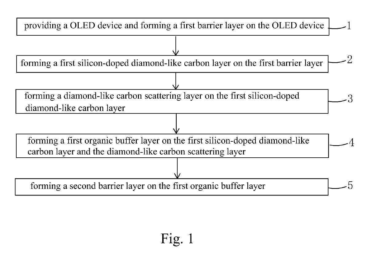
[0048]Referring to FIG. 1, the present invention provides an OLED packaging method, which comprises the following steps:

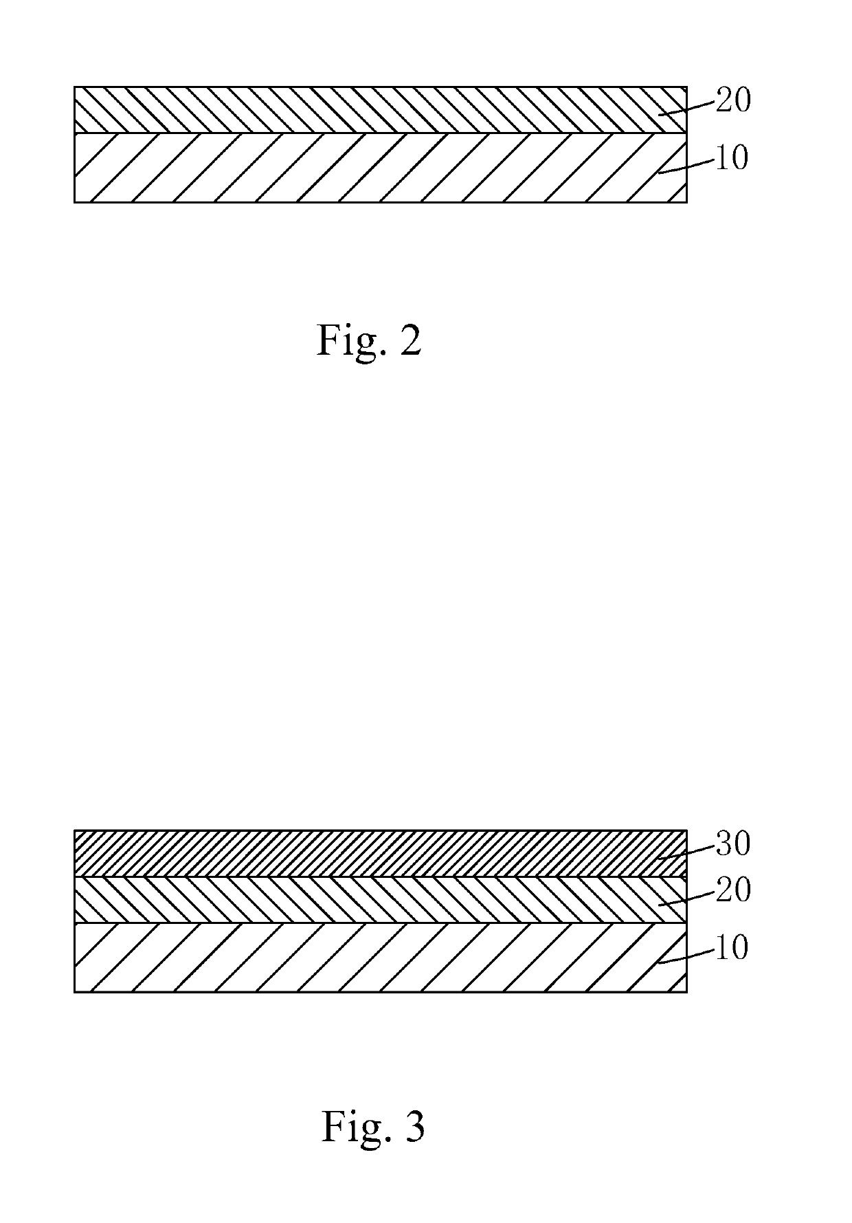
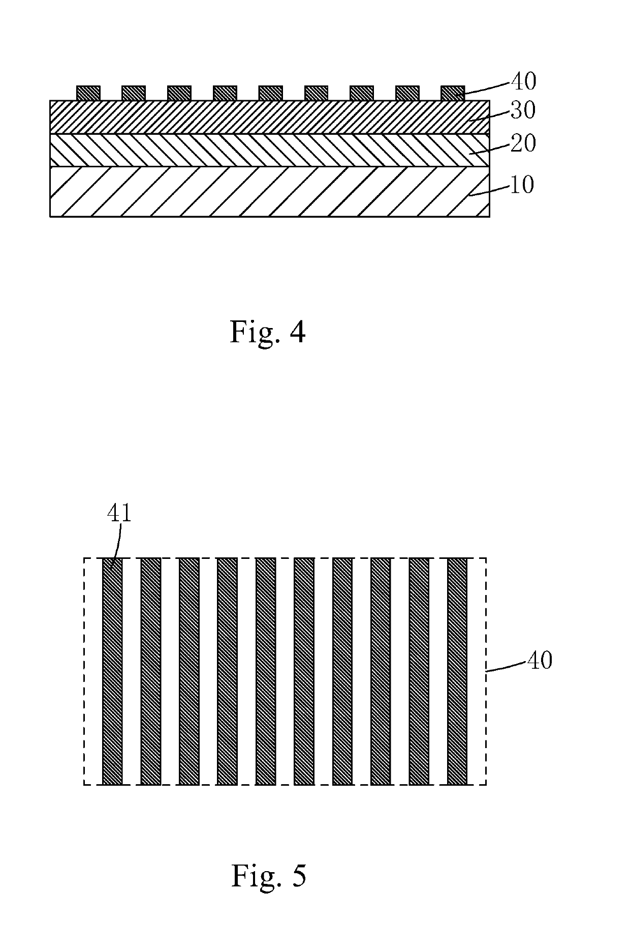
[0049]Step 1: as shown in FIG. 2, providing an OLED device 10 and forming a first barrier layer 20 on the OLED device 10 such that the first barrier layer 20 covers an entire surface of the OLED device 10.

[0050]Specifically, in Step 1, plasma enhanced chemical vapor deposition (PECVD), atomic layer deposition (ALD), pulsed laser deposition (PLD), or sputtering is applied to form the first barrier layer 20.

[0051]Specifically, the first barrier layer 20 is formed of a material comprising one or multiple ones of zirconium aluminate (ZrAlxOy), graphene, aluminum oxide (Al2O3), zirconium oxide (ZrO2), zinc peroxide (ZnO2), silicon nit...


PUM

PropertyMeasurementUnit
thicknessaaaaaaaaaa
refractive indexaaaaaaaaaa
light transmission rateaaaaaaaaaa

Abstract

The present invention provides an OLED packaging method and an OLED package structure. The OLED packaging method of the present invention is such that a silicon-doped diamond-like carbon layer and a diamond-like carbon scattering layer are both provided in an OLED package structure so that the silicon-doped diamond-like carbon layer may provide an effect of blocking external moisture and oxygen and the diamond-like carbon scattering layer is used to provide an effect of increasing light transmission rate, whereby it is possible to greatly extend the service life of the OLED device and also to ensure a relatively high light output efficiency of the OLED device. The OLED package structure of the present invention is such that a silicon-doped diamond-like carbon layer and a diamond-like carbon scattering layer are both provided, so that the silicon-doped diamond-like carbon layer may provide an effect of blocking external moisture and oxygen and the diamond-like carbon scattering layer is used to provide an effect of increasing light transmission rate, whereby it is possible to greatly extend the service life of the OLED device and also to ensure a relatively high light output efficiency of the OLED device.

Description

BACKGROUND OF THE INVENTION[0001]1. Field of the Invention[0002]The present invention relates to the field of display technology, and more particular to an OLED packaging method and an OLED package structure.[0003]2. The Related Arts[0004]Organic light-emitting display (OLED) possesses various advantages, such as being self-luminous, low drive voltage, high luminous efficiency, short response time, high clarity and contrast, almost 180° view angle, wide range of operation temperature, and easy realization of flexible displaying and large-area full-color displaying, and is considered the most promising display device in the industry.[0005]Based on the way of driving, OLEDs can be classified in two categories, passive matrix OLED (PMOLED) and active matrix OLED (AMOLED), namely two categories of direct addressing and TFT array addressing, among which the AMOLED comprises pixels that are arranged in an array and belongs to an active display type, having high light emission performance ...

Claims


Application Information

Patent Timeline
Patent Type & Authority Patents(United States)
IPC IPC(8): H01L51/52H01L51/56
CPCH01L51/5268H01L51/5237H01L51/56H01L51/5253H01L2251/53H01L2251/10H10K50/854H10K50/84H10K71/00H10K2102/302H10K50/844
Inventor JIN, JIANGJIANGHSU, HSIANGLUN
Owner WUHAN CHINA STAR OPTOELECTRONICS TECH CO LTD
Why Eureka
Try Eureka