Supercharge Your Innovation With Domain-Expert AI Agents!

Flexible electronic substrate

a technology of electronic substrates and polymer films, applied in the direction of dielectric characteristics, non-metallic protective coating applications, high frequency circuit adaptations, etc., can solve the problems of limited inability to dissipate heat from electronic devices, and application of flexible electronic substrates based on polymer films. achieve the effect of improving properties

Inactive Publication Date: 2019-05-21
CAMBRIDGE NANOTHERM
View PDF20 Cites 2 Cited by
  • Summary
  • Abstract
  • Description
  • Claims
  • Application Information

AI Technical Summary

Benefits of technology

The nanoceramic layer provides enhanced thermal conductivity and dielectric strength, enabling flexible electronic substrates to manage heat effectively and maintain performance in high-temperature applications, while maintaining flexibility and structural integrity, thus supporting a wide range of electronic devices.

Problems solved by technology

Flexible electronic substrates (FESs) based on polymer films are limited to application in supporting electronic devices that generate low specific heat energy, for example flexible displays, organic light-emitting diodes (OLEDs), key boards, or photovoltaic devices.
Such limitations in the application of FESs are partially due to the low thermal conductivity of polymer films (lower than 1 W / mK), which does not allow dissipation of heat from electronic devices.
Limitations are also partially due to low thermal, structural, and dimensional stability of polymer films.
The presence of natural oxide layer on the surface of some metals (for example Al) can create adhesion problems for traditional deposition coatings or printing techniques.
Anodised Al substrates have not found broad application as FESs because of the inherent low flexibility of the anodised layer.
Anodised layers also have low thermal stability.
Both of these deficiencies lead to formation of micro cracks in the anodic layer, which compromise the dielectric strength of the layer.

Method used


Image

  • Flexible electronic substrate
  • Flexible electronic substrate

Examples


Embodiment Construction

[0059]Preferred embodiments of the invention will now be described with reference to the figures, in which;

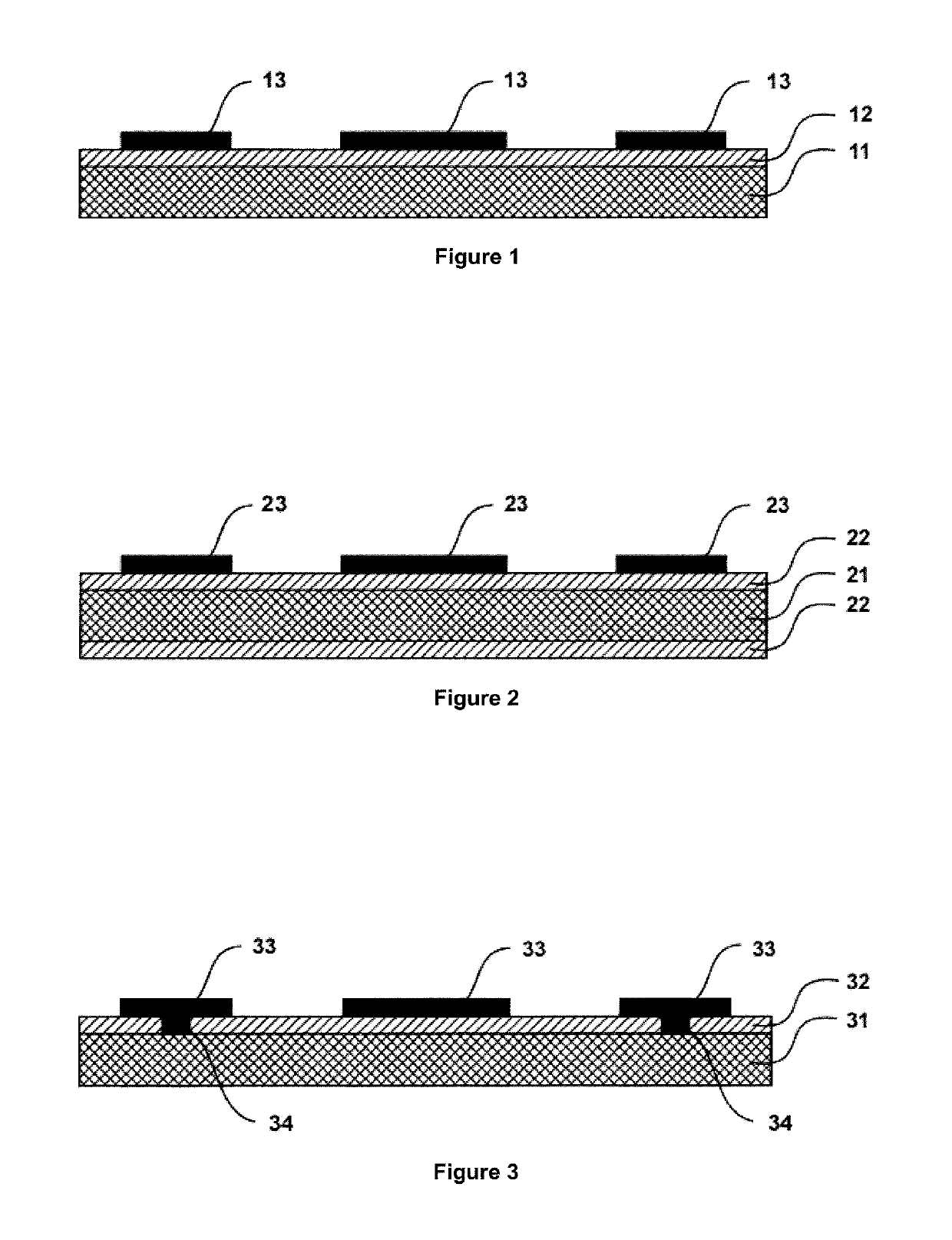
[0060]FIG. 1 is a side view of a FES embodying the invention, which comprises a metallic layer insulated with a dielectric nanoceramic layer applied on one side of metallic layer and an electrical circuit built on the nanoceramic layer;

[0061]FIG. 2 is a side view of a FES embodying the invention, which comprises a metallic layer insulated with dielectric nanoceramic layers applied on both sides of metallic layer and an electrical circuit built on one of the nanoceramic layers;

[0062]FIG. 3 is a side view of a FES embodying the invention, which comprises a metallic layer insulated with a dielectric nanoceramic layer applied on one side of metallic layer and an electrical circuit built on the nanoceramic layer-areas of the electric circuit are connected to the metallic layer by means of conductive vias;

[0063]FIG. 4 is a side view of a FES embodying the invention, which comprises a...


PUM

PropertyMeasurementUnit
thicknessaaaaaaaaaa
thicknessaaaaaaaaaa
thicknessaaaaaaaaaa

Abstract

A flexible electronic substrate (FES) includes a metallic layer, a dielectric nanoceramic layer formed by oxidation of a surface of the metallic layer, and an electrical circuit formed on a surface of the dielectric layer. The FES may be used for supporting a device, for example a flexible display, an OLED, an optoelectronic device, or a rf device. The dielectric nanoceramic layer has a crystalline structure consisting of substantially equiaxed grains having an average grain size of 100 nanometers or less, a thickness of between 1 micrometer and 50 micrometers, a dielectric strength of greater than 20 KV mm−1, and a thermal conductivity of greater than 3 W / mK. The FES has a minimum bend radius of lower than 25 cm.

Description

TECHNICAL FIELD[0001]The invention relates to a flexible electronic substrate (FES), for example a FES for supporting flexible displays, printed batteries, photovoltaic devices, thermoelectric devices, optoelectronic devices, electronic devices, microwave devices, or RF devices.BACKGROUND[0002]Displays, electronic, optoelectronic, microwave, RF, and electrical devices are typically mounted, or printed, on substrates that provide support, arrange electrical power and signal supply, and act to remove heat from the device. Flexible electronic substrates are built on a flexible material base, which normally is a polymer film or metal foil. Flexible electronic substrates (FES) are also named flexible circuits or, flexible PCBs, flex prints or flexi-circuits.[0003]Polymer films are the most common materials used for building FESs and are typically made of a polyester (for example polyethylene terephthalate (PET)), polyimide (PI), polyethylene napthalate (PEN), Polyetherimide (PEI), or one...

Claims


Application Information

Patent Timeline
Patent Type & Authority Patents(United States)
IPC IPC(8): H05K1/02C25D11/02H05K3/44H05K3/28H05K1/03H05K1/05H05K3/00
CPCH05K1/028C25D11/02C25D11/024H05K1/0237H05K1/0306H05K1/053H05K3/28H05K3/44H05K3/0044H05K2203/1147H05K1/05H05K2201/0116H05K2201/0175H05K2203/0315C25D5/18C25D11/04C25D11/26
Inventor SHASHKOV, PAVELUSOV, SERGEY
Owner CAMBRIDGE NANOTHERM
Features
  • R&D
  • Intellectual Property
  • Life Sciences
  • Materials
  • Tech Scout
  • Unparalleled Data Quality
  • Higher Quality Content
  • 60% Fewer Hallucinations
Learn More