Monolithic integration of PMUT on CMOS

a pmut and cmos technology, applied in mechanical vibration separation, instruments, fluid speed measurement, etc., can solve the problems of low fill-factor of the integrated pmut-cmos device, high amount of electrical parasitic, low fill-factor, etc., to reduce the distance between neighboring pmut cells, increase the fill factor, and reduce the path of electrical parasitic.

Active Publication Date: 2019-06-18
SILTERRA MALAYSIA
View PDF5 Cites 20 Cited by
  • Summary
  • Abstract
  • Description
  • Claims
  • Application Information

AI Technical Summary

Benefits of technology

[0023]In this invention, PMUT cells are integrated with the CMOS substrate to form a single unit. Such fabrication technique replaces wire bonding and wafer bonding techniques. In addition, components like bonding ring that occupies a significant space can be eliminated since a separate bonding area is no longer required. The electrical connect that allows adjacent PMUT cells to be electrically connected to each other has a miniature dimension such that it can be positioned within the effective PMUT area. The structure and configuration of PMUT cells on the CMOS substrate increase fill factor and reduce distances between neighboring PMUT cells and lowers the electrical parasitic paths. Further, a single CMOS substrate is only required for accommodating multiple PMUT cells.

Problems solved by technology

However, these bonding methods cause low fill-factor and high amount of electrical parasitic.
When multiple PMUT cells are populated within a specific area, the bond ring and electrical ring occupy significant area and thus causes low fill-factor of the integrated PMUT-CMOS device.

Method used


Image

  • Monolithic integration of PMUT on CMOS
  • Monolithic integration of PMUT on CMOS
  • Monolithic integration of PMUT on CMOS

Examples


Embodiment Construction

[0027]For a better understanding of the invention, preferred embodiments of the invention that are illustrated in the accompanying drawings will be described in detail.

[0028]A monolithic integrated device that integrates a piezoelectric micromachined ultrasonic transducers, PMUT with a complementary metal-oxide-semiconductor, CMOS is introduced in this disclosure. This invention is used in applications for detecting distances, shape or other physical properties of an object through generated waves. The applications include but not limited to medical imaging, fingerprint sensor, industry automation like collision avoidance & non-destructive testing.

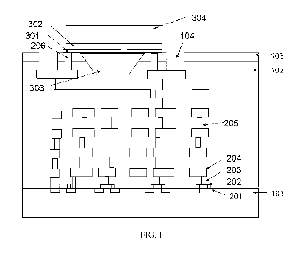
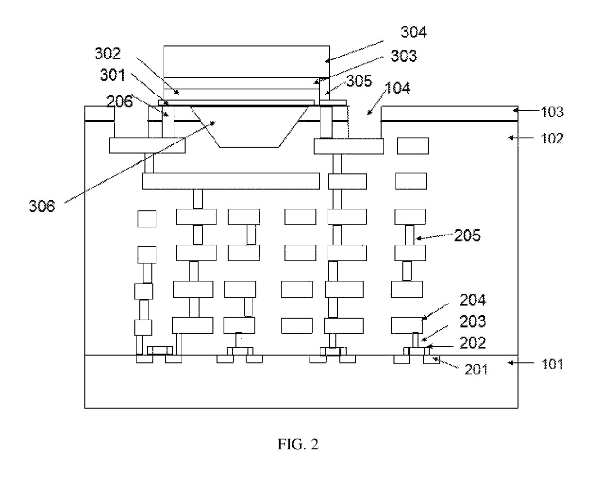
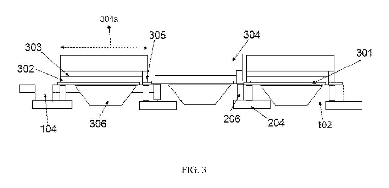
[0029]Referring to FIG. 1 that illustrates the first preferred embodiment of the invention, the monolithic integrated device comprises a substrate layer (101) being the base of the device; an inter-layer dielectric (102) disposed on top of the substrate layer (101) and below a passivation layer (103); an electronic circuitry formed within ...


PUM

PropertyMeasurementUnit
widthaaaaaaaaaa
widthaaaaaaaaaa
elasticaaaaaaaaaa

Abstract

This disclosure describes a monolithic integrated device that comprises a substrate layer being the base of the device, an inter-layer dielectric disposed on top of the substrate layer and below a passivation layer, an electronic circuitry formed within the inter-layer dielectric and supported by the substrate layer, the electronic circuitry comprises a plurality of metal layers formed by one or more spaced apart metals; and at least one micromachined ultrasonic transducer. Each micromachined ultrasonic transducer comprises a bottom electrode disposed on top of the passivation layer and connected to the electronic circuitry, a piezoelectric disposed on top of the bottom electrode, a top electrode disposed on top of the piezoelectric, and an elastic layer positioned on top of the top electrode. There is a cavity formed below the bottom electrode that extends from the passivation layer to a portion of the inter-layer dielectric.

Description

CROSS-REFERENCE TO RELATED APPLICATION[0001]The instant application claims priority to Malaysia Patent Application Ser. No. PI2017703695 filed Sep. 29, 2017, the entire specification of which is expressly incorporated herein by reference.FIELD OF THE INVENTION[0002]This invention relates to a monolithic integrated device. In particular, the device is a monolithic integration of piezoelectric micromachined ultrasonic transducers, PMUT with a complementary metal-oxide-semiconductor, CMOS.BACKGROUND OF THE INVENTION[0003]Micromachined ultrasonic transducer is an electronic device that comprises vibrating membranes capable of generating high pressure waves with an applied AC voltage signal. The generated waves travel through a medium and reflect back to the transducer when the waves meet an object. The transmitted and returned waves are electronically processed to detect information about the object including its distance, shape and other physical properties. The vibration of the membra...

Claims


Application Information

Patent Timeline
Patent Type & Authority Patents(United States)
IPC IPC(8): B81B7/00B06B1/06G01N29/24
CPCB81B7/008B06B1/0644G01N29/2437B81B2201/0271B81B2207/015H01L21/02107H10N30/20H10N30/05H10N30/071B06B1/0674B81C1/00246B81C2203/0735
Inventor SOUNDARA PANDIAN, MOHANRAJKANTIMAHANTI, ARJUN KUMAR
Owner SILTERRA MALAYSIA
Why Eureka
Try Eureka