Supercharge Your Innovation With Domain-Expert AI Agents!

On-chip DC-DC power converters with fully integrated GaN power switches, silicon CMOS transistors and magnetic inductors

a technology of gan power switch and dc-dc power converter, which is applied in the direction of electric variable regulation, process and machine control, instruments, etc., can solve the problems of large converter size and slower transient response, large size of non-integrated structure, and difficulty in achieving high switching frequency and high power density

Inactive Publication Date: 2019-08-27
ELPIS TECH INC
View PDF17 Cites 0 Cited by
  • Summary
  • Abstract
  • Description
  • Claims
  • Application Information

AI Technical Summary

Benefits of technology

The present invention provides a fully integrated DC-DC power converter that includes a silicon-on-insulator (SOI) wafer and magneto-inductor. The process involves selectively removing the SOI layer and buried insulator from the first portion of the SOI wafer, leaving them in the second portion. The second portion of the SOI wafer has a strain relief area and a cavity for optimal performance. The method also includes forming at least one gallium nitride (GaN) transistor and at least one complementary metal-oxide semiconductor (CMOS) transistor on the substrate, depositing a dielectric covering both transistors, and forming at least one magnetic inductor on the dielectric. The technical effect of the invention is an efficient and integrated DC-DC power converter that can be used for on-chip power conversion with improved performance.

Problems solved by technology

However, Si devices have high on-resistance (Ron) and gate capacitance (Cg), and therefore it is challenging for these devices to achieve high switching frequency and high power density.
At the same time, low frequency requires larger passive devices (e.g., inductors), which results in larger converter size and slower transient response.
This non-integrated structure has a big size, has large parasitics, limited switching frequency, and low efficiency.

Method used


Image

  • On-chip DC-DC power converters with fully integrated GaN power switches, silicon CMOS transistors and magnetic inductors
  • On-chip DC-DC power converters with fully integrated GaN power switches, silicon CMOS transistors and magnetic inductors
  • On-chip DC-DC power converters with fully integrated GaN power switches, silicon CMOS transistors and magnetic inductors

Examples


Embodiment Construction

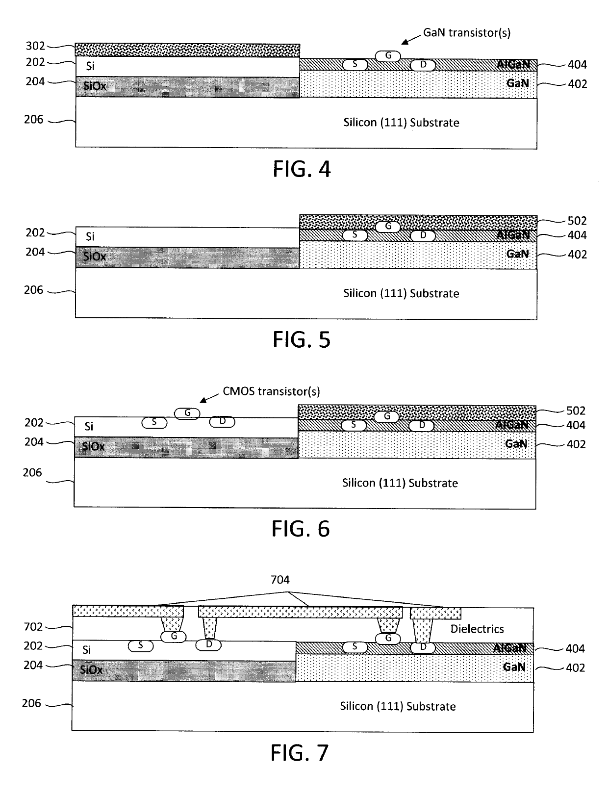
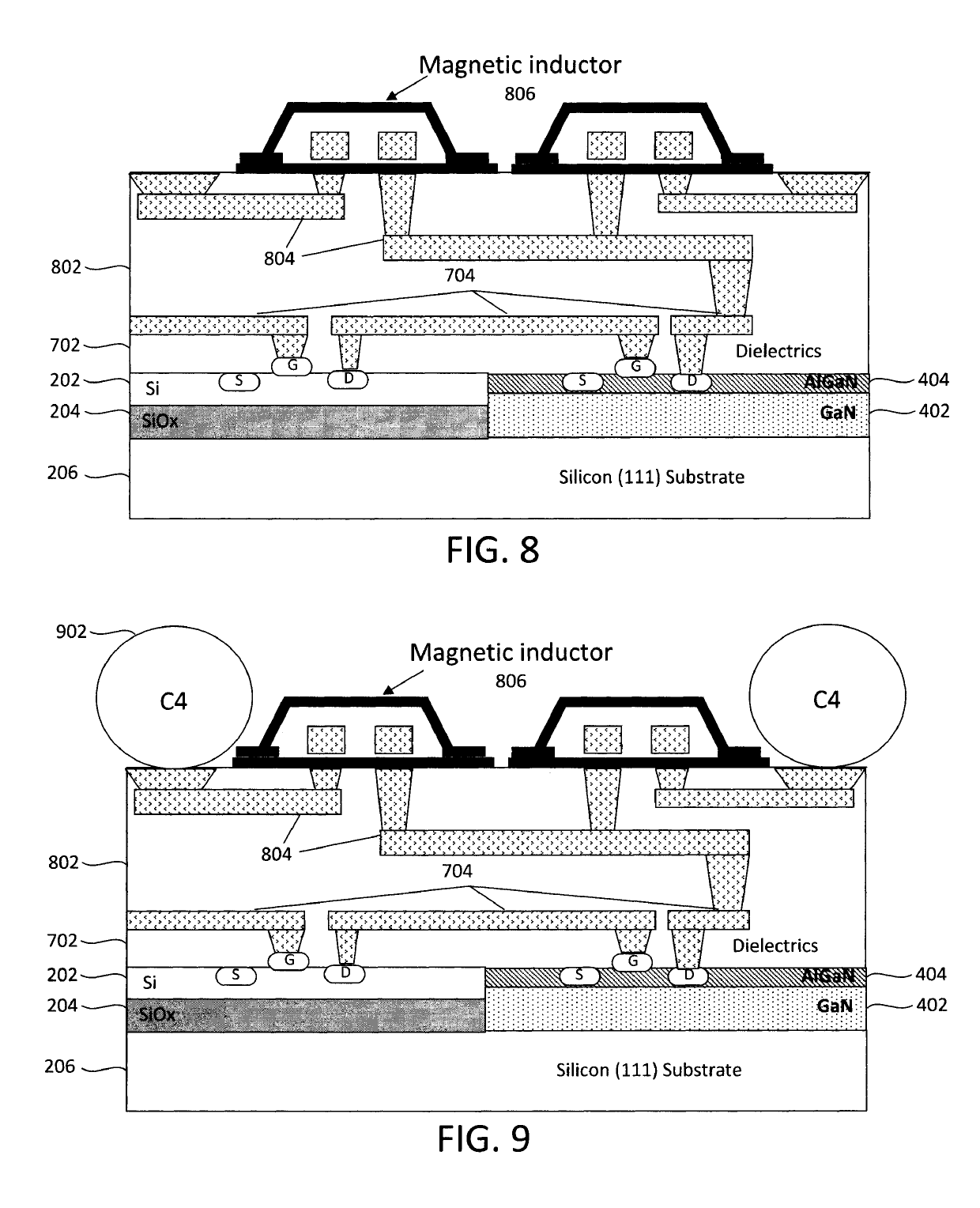
[0024]Provided herein are DC-DC power converter structures with fully integrated GaN switches, magnetic inductors, and CMOS power drivers on a single Si substrate. Some advantages of the present converter design include: 1) a smaller converter size (due to the fully integrated design), 2) high efficiency (due to smaller contact resistance loss from interconnect and bonding wires), 3) low noise (due to smaller parasitic effect from interconnect and bonding wires), 4) fast transient response, and 5) low cost fabrication.

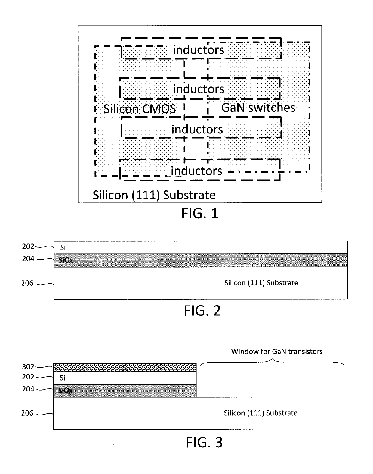
[0025]A top view schematic diagram of an example of the present fully integrated converter design is shown in FIG. 1. In the power converter layout shown in FIG. 1, GaN transistors (GaN switches) and CMOS transistors (silicon CMOS) are fully integrated on the front-end-of-line (FEOL) with magnetic inductors (inductors) on the back-end-of-line (BEOL) of a common chip.

[0026]An exemplary methodology for fabricating the DC-DC power converter design of FIG. 1 is now describ...


PUM


Abstract

Fully integrated, on-chip DC-DC power converters are provided. In one aspect, a DC-DC power converter includes: a SOI wafer having a SOI layer separated from a substrate by a buried insulator, wherein the SOI layer and the buried insulator are selectively removed from at least one first portion of the SOI wafer, and wherein the SOI layer and the buried insulator remain present in at least one second portion of the SOI wafer; at least one GaN transistor formed on the substrate in the first portion of the SOI wafer; at least one CMOS transistor formed on the SOI layer in the second portion of the SOI wafer; a dielectric covering the GaN and CMOS transistors; and at least one magnetic inductor formed on the dielectric. A method of forming a fully integrated DC-DC power converter is also provided.

Description

CROSS-REFERENCE TO RELATED APPLICATION(S)[0001]This application is a continuation of U.S. application Ser. No. 15 / 185,807 filed on Jun. 17, 2016, now U.S. Pat. No. 9,806,615, the disclosure of which is incorporated by reference herein.FIELD OF THE INVENTION[0002]The present invention relates to direct current (DC)-DC power converters, and more particularly, to fully integrated, on-chip DC-DC power converters.BACKGROUND OF THE INVENTION[0003]A switched-inductor power converter is the most widely used DC-DC power converter topology in power electronics due to its high efficiency, variable conversion ratio, and power-handling ability. A Buck DC-DC power converter can be used to step down voltage from its input / supply to its output / load. Thus Buck converters are also referred to as step-down converters. In Buck converters, an inductor is used to store energy and two switches are used to control the currents flowing in the inductors.[0004]It is desirable for DC-DC power converters to wor...

Claims


Application Information

Patent Timeline
Patent Type & Authority Patents(United States)
IPC IPC(8): H01L21/00H01L21/768H02M3/158H01L29/00H01L27/00H01L29/201H01L23/535H01L21/762H01L21/84H02M3/00H01L23/522H01L21/8258H01L27/12H01L23/00H01L27/085
CPCH01L2224/05569H01L21/8258H01L23/5227H01L24/13H01L27/085H01L27/1207H01L2224/0401H01L2224/131H01L2924/10253H01L2924/1033H01L2924/19104H01L21/7624H01L21/84Y02B70/10H02M3/003H01L2924/014H01L2924/00014H01L21/76895H01L21/76243H01L23/535H01L29/201H01L27/1203H02M3/158
Inventor DELIGIANNI, HARIKLIASADANA, DEVENDRA K.SPROGIS, EDMUND J.WANG, NAIGANG
Owner ELPIS TECH INC
Features
  • R&D
  • Intellectual Property
  • Life Sciences
  • Materials
  • Tech Scout
  • Unparalleled Data Quality
  • Higher Quality Content
  • 60% Fewer Hallucinations
Learn More