Liquid crystal display device

a liquid crystal display and active matrix technology, applied in semiconductor devices, instruments, optics, etc., can solve the problems of increasing the number of power supply lines, increasing the power consumption of the display device, and complicating the method, so as to reduce the number of times of writing image signals in a certain period, the effect of low off-state current and less change in transmittan

Inactive Publication Date: 2019-09-17
SEMICON ENERGY LAB CO LTD
View PDF193 Cites 4 Cited by
  • Summary
  • Abstract
  • Description
  • Claims
  • Application Information

AI Technical Summary

Benefits of technology

[0010]For wide viewing angle and high-speed response, the liquid crystal drive device disclosed in Patent Document 1 uses three electrodes to control liquid crystal molecules. However, even when high-speed response can be achieved, the three electrodes need to be driven separately, which increases the power consumption of the display device.
[0011]In the liquid crystal drive device disclosed in Patent Document 2, two pairs of electrodes, that is, four electrodes are used to drive liquid crystal and at least four power supply lines are needed; thus, there is a problem in that the number of power supply lines is increased. The increase in the number of power supply lines complicates a method for driving or controlling voltage applied to the liquid crystal and increases power consumption.
[0012]In view of the above technical background, an object of one embodiment of the present invention is to provide a liquid crystal display device with low power consumption. Another object of one embodiment of the present invention is to provide a liquid crystal display device in which change in transmittance is reduced. Another object of one embodiment of the present invention is to provide a liquid crystal display device in which change in display luminance is reduced. Another object of one embodiment of the present invention is to provide a liquid crystal display device in which flickers of display are reduced. Another object of one embodiment of the present invention is to provide a liquid crystal display device capable of eye-friendly display. Another object of one embodiment of the present invention is to provide a liquid crystal display device that causes less eye fatigue.
[0014]In a liquid crystal display device of one embodiment of the present invention, an insulated-gate field-effect transistor (hereinafter, simply referred to as a transistor) with extremely low off-state current is provided in a pixel in order to keep display of images on a pixel portion after the writing of image signals to the pixel portion is stopped. By using the above transistor as an element for controlling the supply of voltage to a liquid crystal element included in the pixel, the voltage applied to the liquid crystal element can be held for a long time. Thus, for example, in the case where image signals having the same image data are repeatedly written to the pixel portion during continuous frame periods as in the case of displaying a still image, the displayed image can be maintained even when the driving frequency is lowered by temporarily stopping the writing of image signals to the pixel portion, that is, even when the number of times of writing of image signals in a certain period is reduced.
[0015]In the liquid crystal display device of one embodiment of the present invention, a liquid crystal element includes a liquid crystal layer to which an electric field is applied by three electrodes (a pixel electrode, a first common electrode, and a second common electrode). A negative liquid crystal material is used for the liquid crystal layer. The specific resistivity of the liquid crystal material is greater than or equal to 1.0×10¹³ Ω·cm and less than or equal to 1.0×10¹⁶ Ω·cm. With this structure, the liquid crystal display device causes less change in transmittance and few image flickers perceivable by users even when the number of image signal writing operations in a certain period is reduced.
[0016]One embodiment of the present invention can provide a liquid crystal display device with low power consumption. Another embodiment of the present invention can provide a liquid crystal display device with less change in transmittance.

Problems solved by technology

However, even when high-speed response can be achieved, the three electrodes need to be driven separately, which increases the power consumption of the display device.
In the liquid crystal drive device disclosed in Patent Document 2, two pairs of electrodes, that is, four electrodes are used to drive liquid crystal and at least four power supply lines are needed; thus, there is a problem in that the number of power supply lines is increased.
The increase in the number of power supply lines complicates a method for driving or controlling voltage applied to the liquid crystal and increases power consumption.

Method used


Image

  • Liquid crystal display device
  • Liquid crystal display device
  • Liquid crystal display device

Examples


embodiment 1

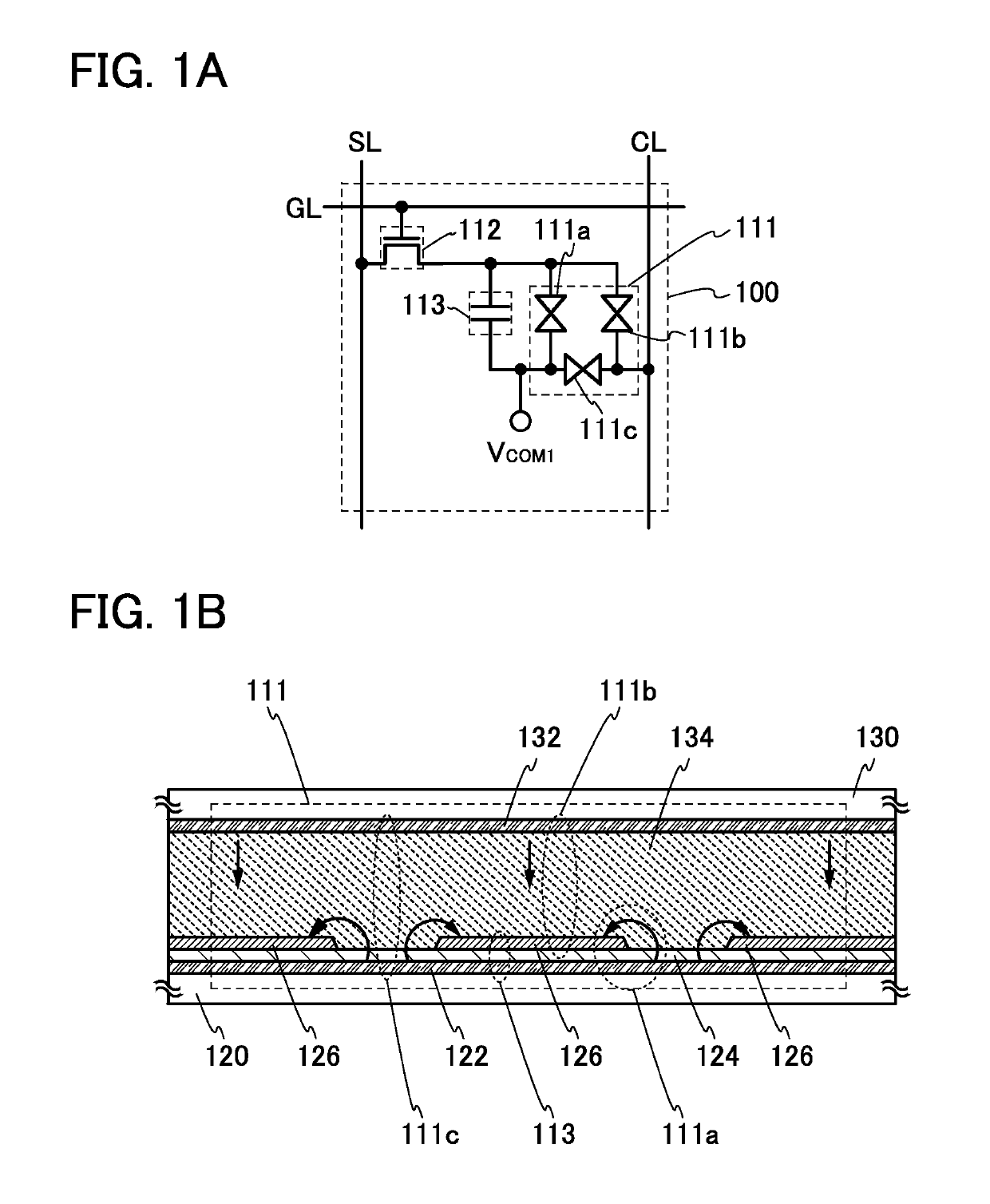
[0043]In this embodiment, a configuration example of a pixel in a liquid crystal display device of one embodiment of the present invention is described with reference to FIGS. 1A and 1B.

[0044]FIG. 1A illustrates a configuration example of a pixel included in the liquid crystal display device of one embodiment of the present invention. A pixel 100 illustrated in FIG. 1A includes a liquid crystal element 111, a transistor 112 controlling the supply of an image signal to the liquid crystal element 111, and a capacitor 113.

[0045]The liquid crystal element 111 includes a pixel electrode, a first common electrode, a second common electrode, and a liquid crystal layer which contains a liquid crystal material and to which a voltage is applied across the pixel electrode, the first common electrode, and the second common electrode.

[0046]In the liquid crystal element 111 illustrated in FIG. 1A, a region where voltage is applied between the pixel electrode and the first common electrode is deno...

embodiment 2

[0150]In this embodiment, an oxide semiconductor film that can be used in the liquid crystal display device of one embodiment of the present invention is described.

[0151]A highly purified oxide semiconductor (a purified OS) obtained by reduction of impurities such as moisture or hydrogen that serve as electron donors (donors) and reduction of oxygen vacancies is an intrinsic (i-type) semiconductor or a substantially intrinsic semiconductor. Thus, a transistor including a channel formation region in a highly purified oxide semiconductor film has extremely low off-state current and high reliability.

[0152]Specifically, various experiments can prove low off-state current of a transistor including a channel formation region in a highly purified oxide semiconductor film. For example, even when an element has a channel width of 1×106 μm and a channel length of 10 μm, off-state current can be lower than or equal to the measurement limit of a semiconductor parameter analyzer, i.e., lower tha...

embodiment 3

[0213]In this embodiment, a configuration example of a pixel in a liquid crystal display device of one embodiment of the present invention, which is different from the pixel 100 illustrated in the top view of FIG. 5 and the cross-sectional view of FIG. 6 in Embodiment 1, is described with reference to FIG. 10 and FIG. 11.

[0214]FIG. 10 is an example of a top view of the pixel 100 illustrated in FIG. 1A. In FIG. 10, some components (e.g., a gate insulating film) are not illustrated for clarity of the top view of the pixel 100. FIG. 11 is a cross-sectional view taken along the dashed-dotted line A1-A2 and the dashed-dotted line A3-A4 in FIG. 10.

[0215]In the pixel 100 illustrated in FIG. 10 and FIG. 11, a conductive film 304 serving as the gate of the transistor 112 and the wiring GL is provided over the substrate 302 having an insulating surface. In addition, an electrode 354 serving as an electrode of the capacitor 113 and the first common electrode is provided over the substrate 302....


PUM

PropertyMeasurementUnit
specific resistivityaaaaaaaaaa
frequencyaaaaaaaaaa

Abstract

The liquid crystal display device includes a first substrate, a second substrate, and a liquid crystal layer between the first substrate and the second substrate. The first substrate includes a transistor including an oxide semiconductor film including a channel formation region; a pixel electrode electrically connected to the transistor; an insulating layer in contact with the pixel electrode; and a first common electrode in contact with the insulating layer. The second substrate faces the first substrate and includes a second common electrode. A negative liquid crystal material is used for the liquid crystal layer. The specific resistivity of the liquid crystal material is greater than or equal to 1.0×10¹³ Ω·cm and less than or equal to 1.0×10¹⁶ Ω·cm.

Description

BACKGROUND OF THE INVENTION[0001]1. Field of the Invention[0002]The present invention relates to, for example, a semiconductor device, a display device, a light-emitting device, a driving method thereof, or a manufacturing method thereof. In particular, the present invention relates to, for example, an active matrix liquid crystal display device.[0003]2. Description of the Related Art[0004]With the recent rapid spread of portable information terminals such as smartphones, improvement in their performance has progressed rapidly. Their screens have been increased in size and resolution. In addition to improvement in the resolution of a screen, emphasis has been put on power consumption of a display device. A typical example of the display device is a liquid crystal display device using liquid crystal elements.[0005]Examples of display modes for the liquid crystal display device include a vertical alignment (VA) mode in which liquid crystal molecules with negative dielectric constant a...

Claims


Application Information

Patent Timeline
Patent Type & Authority Patents(United States)
IPC IPC(8): G02F1/1343G02F1/137H01L27/12
CPCG02F1/134363G02F2001/134372H01L27/1225G02F2001/13712G02F2001/134381G02F1/134381G02F1/134372G02F1/13712G02F1/136213
Inventor HATSUMI, RYOFUKAI, SHUJIKUBOTA, DAISUKE
Owner SEMICON ENERGY LAB CO LTD
Why Eureka
Try Eureka