Magnetoresistance effect device and high frequency device

a magnetoresistance effect and high frequency technology, applied in the field of magnetoresistance effect devices and high frequency devices, can solve the problems of insufficient investigation of other applications of ferromagnetic resonance phenomena, and achieve the effect of increasing the change rate of magnetoresistance of the magnetoresistance effect element 10 and high spin polarizability

Active Publication Date: 2019-10-08
TDK CORPARATION
View PDF9 Cites 1 Cited by
  • Summary
  • Abstract
  • Description
  • Claims
  • Application Information

AI Technical Summary

Benefits of technology

[0035]The magnetoresistance effect element 10 includes a magnetization fixed layer 11, a magnetization free layer 12, and a spacer layer 13. The spacer layer 13 is located between the magnetization fixed layer 11 and the magnetization free layer 12. It is more difficult for magnetization of the magnetization fixed layer 11 to move in comparison with magnetization of the magnetization free layer 12 and it is fixed in one direction under a predetermined magnetic field environment. A direction of the magnetization of the magnetization free layer 12 is changed relative to the direction of the magnetization of the magnetization fixed layer 11 to achieve a function of the magnetoresistance effect element 10.
[0036]The magnetization fixed layer 11 is formed of a ferromagnetic material. It is preferable for the magnetization fixed layer 11 to be formed of a material having a high spin polarizability, such as Fe, Co, Ni, an alloy of Ni and Fe, an alloy of Fe and Co, or an alloy of Fe and Co and B. Using such a material, a change rate of magnetoresistance of the magnetoresistance effect element 10 is increased. Further, the magnetization fixed layer 11 may be formed of a Heusler alloy. It is preferable for a thickness of the magnetization fixed layer 11 to be 1 to 10 nm.
[0037]A method of fixing the magnetization of the magnetization fixed layer 11...

Problems solved by technology

However, specific investigation of other applications of...

Method used


Image

  • Magnetoresistance effect device and high frequency device
  • Magnetoresistance effect device and high frequency device
  • Magnetoresistance effect device and high frequency device

Examples


first embodiment

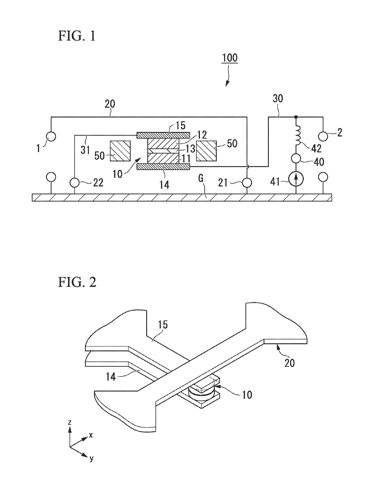
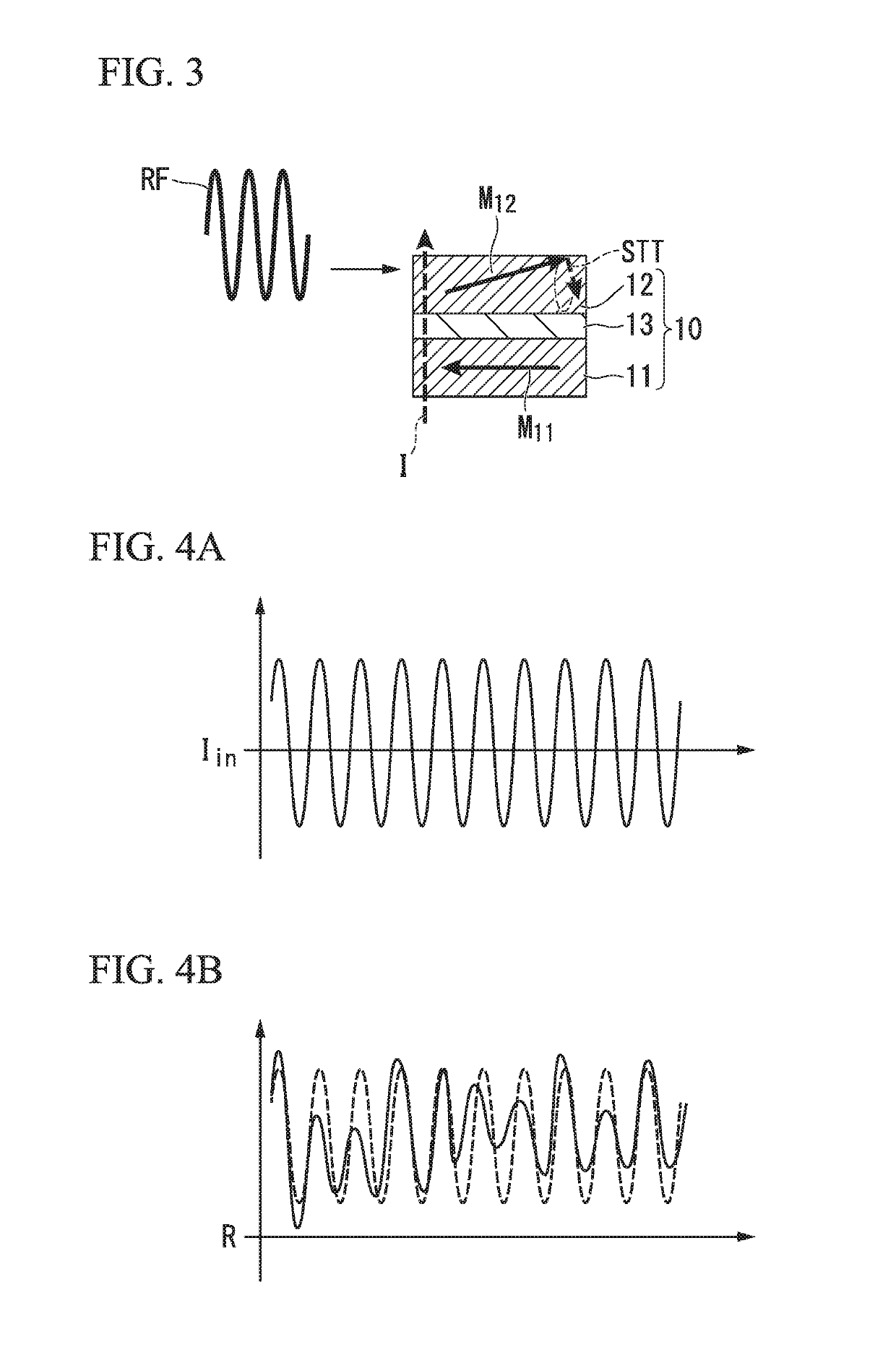
[0032]FIG. 1 is a schematic diagram showing a circuit configuration of a magnetoresistance effect device according to a first embodiment of the present disclosure. The magnetoresistance effect device 100 shown in FIG. 1 includes a magnetoresistance effect element 10, a first signal line 20, and a DC application terminal 40. The magnetoresistance effect device 100 receives a signal from a first port 1 and outputs a signal from a second port 2. The signal to be output can be changed by a frequency setting apparatus 50.

[0033]The first port 1 is an input terminal of the magnetoresistance effect device 100. The first port 1 corresponds to one end of the first signal line 20. An AC signal source (not shown) is connected to the first port 1, and an AC signal (a high frequency signal) can be applied to the magnetoresistance effect device 100. The high frequency signal applied to the magnetoresistance effect device 100 is, for example, a signal having a frequency of 100 MHz or more.

[0034]The...

second embodiment

[0109]FIG. 8 is a diagram schematically showing a circuit configuration of the magnetoresistance effect device 101 according to a second embodiment. The magnetoresistance effect device 101 according to the second embodiment is different from the magnetoresistance effect device 100 according to the first embodiment in that there are a plurality of magnetoresistance effect elements 10, which are connected in parallel to each other. The other constituents are the same, and constituents which are the same are denoted with the same reference numerals.

[0110]The magnetoresistance effect device 101 shown in FIG. 8 includes a first magnetoresistance effect element 10a and a second magnetoresistance effect element 10b. The first magnetoresistance effect element 10a and the second magnetoresistance effect element 10b are connected in parallel to the second port 2 and the power supply 41. A DC current or a DC voltage is applied from the power supply 41 to the first magnetoresistance effect elem...

third embodiment

[0114]FIG. 10 is a diagram schematically showing a circuit configuration of a magnetoresistance effect device 103 according to a third embodiment. The magnetoresistance effect device 103 according to the third embodiment is different from the magnetoresistance effect device 100 according to the first embodiment in that there are a plurality of magnetoresistance effect elements 10, which are connected in series. The other constituents are the same, and constituents which are the same are denoted with the same reference numerals.

[0115]In the magnetoresistance effect device 103 shown in FIG. 10, a first magnetoresistance effect element 10a and a second magnetoresistance effect element 10b are connected in series in a closed circuit formed of a power supply 41, an output signal line 30, a line 31, and a ground G ADC current or a DC voltage is applied from the power supply 41 to the first magnetoresistance effect element 10a and the second magnetoresistance effect element 10b and, in eit...


PUM


Abstract

A magnetoresistance effect device includes a magnetoresistance effect element including a magnetization fixed layer, a magnetization free layer of which a direction of magnetization is changeable relative to a direction of magnetization of the fixed layer, and a spacer layer sandwiched between the fixed and free layers, a first signal line configured to generate a high frequency magnetic field when a high frequency current flows and apply the field to the magnetization free layer, and a DC application terminal configured to be capable of connecting a power supply for applying a DC current or voltage in a stacking direction of the element, and the element is disposed with respect to the terminal so the DC current flows from the fixed layer to the free layer in the element or so the DC voltage at which the magnetization fixed layer is higher in potential than the magnetization free layer is applied.

Description

BACKGROUND[0001]The disclosure relates to a magnetoresistance effect device and a high frequency device.[0002]Priority is claimed on Japanese Patent Application No. 2017-152725, filed Aug. 7, 2017, the content of which is incorporated herein by reference.[0003]In recent years, as mobile communication terminals such as cellular phones have become more sophisticated, the speed of wireless communication has increased. Since the communication speed is proportional to a bandwidth of a frequency to be used, a frequency band required for communication is becoming larger. In addition, the required number of high frequency filters mounted on mobile communication terminals is also increasing.[0004]Further, in recent years, spintronics has been studied as a field likely to be applied to new high frequency parts. One of phenomena attracting attention in the field is a ferromagnetic resonance phenomenon due to a magnetoresistance effect element (see Non-Patent Document, J.-M. L. Beaujour, et al....

Claims


Application Information

Patent Timeline
IPC IPC(8): H03H11/04H01F10/32H03H2/00H03F15/00H03H11/16
CPCH03H2/00H03F15/00H03H11/04H01F10/329H03H11/16H01F10/3286H01L23/66H01L25/04H10N50/80H10N50/10
Inventor DEGAWA, NAOMICHIYAMANE, TAKEKAZU
Owner TDK CORPARATION
Why Eureka
Try Eureka