III-V or II-VI compound semiconductor films on graphitic substrates

a technology of compound semiconductor films and graphitic substrates, which is applied in the direction of crystal growth process, polycrystalline material growth, chemically reactive gases, etc., can solve the problems of high cost, high limit, and inability to use the same material as a substrate, and achieve the effect of enhancing the epitaxial growth of films

Active Publication Date: 2019-11-12
NORWEGIAN UNIVERSITY OF SCIENCE AND TECHNOLOGY (NTNU)
View PDF29 Cites 2 Cited by
  • Summary
  • Abstract
  • Description
  • Claims
  • Application Information

AI Technical Summary

Benefits of technology

[0044]Having a film grown epitaxially provides homogeneity to the formed material which may enhance various end properties, e.g. mechanical, optical or electrical properties.
[0132]An ideal device for their deployment might be a thin film solar cell. Such solar cell has the potential to be efficient, cheap and lightweight at the same time. This is a rapidly developing field and further applications on these valuable materials will be found in the next years.

Problems solved by technology

Using the same material as a substrate is, however, also highly limiting.
Also, the necessary substrate materials may be expensive.
That can be difficult and adds to the expense of the substrate.
These dislocation rich layers are of limited interest as semiconductors.
However, the necessary substrate materials for heteroepitaxial growth may not be readily available and they may again be expensive.
Without this lattice match, a useful film does not form.

Method used


Image

  • III-V or II-VI compound semiconductor films on graphitic substrates
  • III-V or II-VI compound semiconductor films on graphitic substrates
  • III-V or II-VI compound semiconductor films on graphitic substrates

Examples


example 1

[0143]After annealing the graphene substrate at 550° C., the substrate temperature is then decreased to typically between 200° C. and 300° C. for Sb deposition. Sb flux is first supplied to the surface during a time interval typically in the range 5 s to 1 minute, dependent on Sb flux and substrate temperature. A few nm, preferably less than a few tens of nm, of Sb are then grown, preferably by MEE or ALMBE. Then, the substrate temperature is increased to a temperature suitable for GaSb thin film growth: i.e. around 450° C. The temperature of the Ga effusion cell is preset to yield a nominal planar growth rate of 0.3 μm per hour. The Sb2 flux is set to 1×10⁻⁶ Torr to grow the GaSb thin film at this temperature. The GaSb thin film is doped to a level appropriate for which device structure will be grown on top of this thin film template structure.

example 2

[0144]After annealing the graphene substrate at 550° C., the substrate temperature is decreased to between 15° C. and 80° C. for As deposition, the temperature being dependent on which deposition rate is wanted. As flux is first supplied to the surface during a time interval typically in the range 5 s to 1 minute. A few nm, preferably less than a few tens of nm, InAs are then grown, preferably by MEE or ALMBE. Then, the substrate temperature is increased to a temperature suitable for InAs thin film growth: i.e. around 450° C. The temperature of the In effusion cell is preset to yield a nominal planar growth rate of up to 0.7 μm per hour. The As2 flux is set to 6×10⁻⁶ Torr to form the InAs thin film at this temperature. The InAs thin film is doped to a level appropriate for which device structure will be grown on top of this thin film template structure.

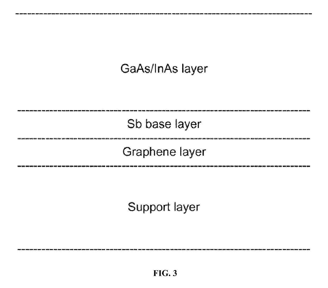
[0145]The substrates prepared in examples 1 and 2 hereby called as III-V / GP thin film substrate can be used as a template for the fa...

example 3

[0147]p-i-n doped homojunction GaSb thin film is further grown on III-V / GP thin film substrate of example 1 to use it as a photodetector. The thickness of each of the p-doped, n-doped, and intrinsic III-V epilayer is typically kept between 0.5 and 3 μm. For p-type doping, Be is used. Te is used as an n-dopant. The Be cell temperature is set to 990° C. which gives a nominal p-type doping concentration of 3×1018 cm−3. The Te cell temperature is set to 440° C. which gives a nominal n-type doping concentration of 1×1018 cm−3. The deposition temperature for all the layers is set to 450° C. The temperature of the Ga effusion cell is preset to yield a nominal planar growth rate of 0.7 μm per hour, and the Sb2 flux is set to 1×10⁻⁶ Torr to grow the GaSb thin film.


PUM

PropertyMeasurementUnit
thicknessaaaaaaaaaa
thicknessaaaaaaaaaa
interplanar spacingaaaaaaaaaa

Abstract

A composition of matter comprising a film on a graphitic substrate, said film having been grown epitaxially on said substrate, wherein said film comprises at least one group III-V compound or at least one group II-VI compound.

Description

[0001]This invention concerns a process for growing thin films epitaxially on graphitic substrates. In particular, the invention employs molecular beam epitaxy techniques to grow semiconducting thin films epitaxially on graphitic substrates. The resulting graphite supported semiconducting films form a further aspect of the invention. The films are preferably semiconductor materials and have wide ranging applications in, for example, the electronics industry or in solar cell applications.[0002]Over recent years, the interest in semiconductors has intensified as nanotechnology becomes an important engineering discipline. Semiconductor technology has found important applications in a variety of electrical devices such as sensors, solar cells and LED's.[0003]Many different types of semiconductors are known, some in film form. Conventionally, semiconductor films have been grown on a substrate identical to the semiconductor itself (homoepitaxial growth) Thus, GaAs was grown on GaAs, Si on...

Claims


Application Information

Patent Timeline
Patent Type & Authority Patents(United States)
IPC IPC(8): C30B25/10C30B29/48H01L29/22H01L29/20H01L29/04H01L29/15H01L29/16C30B29/02C30B29/40C30B25/18H01L21/02
CPCH01L21/02551H01L21/02466H01L21/02455C30B29/48C30B25/105H01L29/1606H01L21/02376H01L29/151H01L29/20H01L29/22C30B29/40C30B25/183H01L21/02631C30B29/02H01L29/045H01L29/16H01L21/02485H01L21/02469H01L21/02538Y02E10/544
Inventor FIMLAND, BJØRN-OVEDASA, DHEERAJ L.WEMAN, HELGE
Owner NORWEGIAN UNIVERSITY OF SCIENCE AND TECHNOLOGY (NTNU)
Why Eureka
Try Eureka