Unlock instant, AI-driven research and patent intelligence for your innovation.

Multi-layer circuit board and manufacturing method thereof

a multi-layer circuit board and manufacturing method technology, applied in the field of circuit boards, can solve the problems of high post-treatment pollution, complex process, and lower final product yield, and achieve the effect of preventing bumps from skewing and improving material properties

Active Publication Date: 2019-12-03
WINBOND ELECTRONICS CORP
View PDF12 Cites 0 Cited by
  • Summary
  • Abstract
  • Description
  • Claims
  • Application Information

AI Technical Summary

Benefits of technology

The invention is a process of making a multi-layer circuit board using a non-metal material to create bumps on the board. This improves the material properties of the board and prevents the bumps from getting distorted during the pressing and puncturing process. The process involves printing the bumps with a ceramic-like material using 3D printing, and then printing the conductive circuit on top of the bumps using a different 3D printing technique. This simplifies the fabrication process and allows for more efficient use of the material. The non-metal material used to pre-fabricate the bumps also provides better material properties, reduces material consumption, and helps reduce pollution in the environment.

Problems solved by technology

The method has disadvantages of complex process, high pollution post-treatment, and lower yield of final products.
However, in the B2it process, since a conductive paste used to fabricate the bumps has material properties of high viscosity and low thixotropic index (TI), only performing one time of printing on the conductive material is unable to reach the design height.
Additionally, in the process that the bumps puncture the insulation laminate board to superimposed build-up layers, the conductive bumps are prone to skew, which will cause bad conductive connection of a printed circuit board (PCB), thereby reducing the production yield.

Method used


Image

  • Multi-layer circuit board and manufacturing method thereof
  • Multi-layer circuit board and manufacturing method thereof
  • Multi-layer circuit board and manufacturing method thereof

Examples


Embodiment Construction

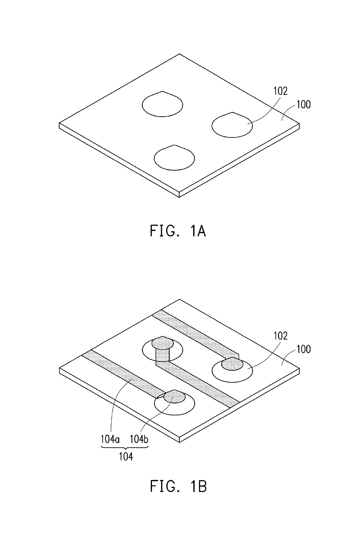
[0014]Referring to FIG. 1A, a substrate 100 is provided first. The substrate 100 includes an insulating substrate, and a material thereof is a resin, for example. Then, a plurality of insulation bumps 102 are formed on the substrate 100. A hardness of the insulation bump is larger than that of silver, for example. That is, the hardness of the insulation bump is larger than Mohs hardness of 2.7, for example. A material of the insulation bump 102 includes a ceramic-like material, such as zirconium oxide, aluminum oxide, silicon dioxide, titanium dioxide, silicon nitride, silicon carbide, or a combination thereof. The insulation bumps 102 are formed by a 3D printing method, for example. The ceramic-like material powder is printed to a bump shape by a 3D printing technique. Additionally, after forming the plurality of insulation bumps 102 using the 3D printing technique, a sintering process may be performed to sinter the ceramic-like powder to a ceramic body. In an embodiment, the plura...


PUM

PropertyMeasurementUnit
conductiveaaaaaaaaaa
sizeaaaaaaaaaa
insulatingaaaaaaaaaa

Abstract

A multi-layer circuit board including a plurality of insulation bumps, a first conductive layer, and a second conductive layer is provided. The plurality of insulation bumps are disposed between a first substrate and a second substrate. A top portion of the plurality of insulation bumps is served as a circuit connection point. The first conductive layer is disposed on the first substrate and connected to the circuit connection point. The second conductive layer is disposed on the second substrate and connected to the circuit connection point.

Description

CROSS-REFERENCE TO RELATED APPLICATION[0001]This application claims the priority benefit of China application serial no. 201611107853.0, filed on Dec. 6, 2016. The entirety of the above-mentioned patent application is hereby incorporated by reference herein and made a part of this specification.BACKGROUND OF THE INVENTIONField of the Invention[0002]The invention relates to a circuit board, and particularly relates to a multi-layer circuit board using a 3D printing technique and a manufacturing method thereof.Description of Related Art[0003]To achieve high-density circuit design and high density circuit interlayer interconnection, it is necessary to reduce circuit using space occupied by vias in a normal circuit board. A manufacturing method of an interlayer interconnection technique commonly used for a high density interconnection (HDI) is a free stacked via structure which uses processes of laser drilling and metal hole filling to complete the electrical connection of the circuit i...

Claims


Application Information

Patent Timeline
Patent Type & Authority Patents(United States)
IPC IPC(8): H05K1/11H05K1/03H05K1/14H05K3/46H05K3/00H05K3/12B33Y80/00H05K3/40
CPCH05K3/0014H05K1/0306H05K3/12H05K1/115H05K1/111H05K3/4629H05K3/4664H05K3/4614H05K1/14B33Y80/00H05K3/403H05K2201/09045H05K1/0298H05K1/119H05K3/4644Y10T29/49155
Inventor CHEN, YU-MING
Owner WINBOND ELECTRONICS CORP