

Thallium bromide (TIBr) semiconductors and devices with extended life apparatus, methods, and system
a technology of thallium bromide and extended life, which is applied in the field of thallium bromide (tibr) semiconductors and devices with extended life apparatus, methods and systems, can solve the problems of limiting the operable lifetime of a device, insufficient electro-migration of thermal and/or impurity-generated cation and anion vacancies in the crystalline structure of tlbr devices, and insufficient to account for observed aging rates in thos
- Summary
- Abstract
- Description
- Claims
- Application Information
AI Technical Summary
Benefits of technology
Problems solved by technology
Method used
Image

Examples
Embodiment Construction
[0002]This invention was made with Government support under Contract No. DE-NA0003525 awarded by the United States Department of Energy / National Nuclear Security Administration. The U.S. Government has certain rights in the invention.
BACKGROUND
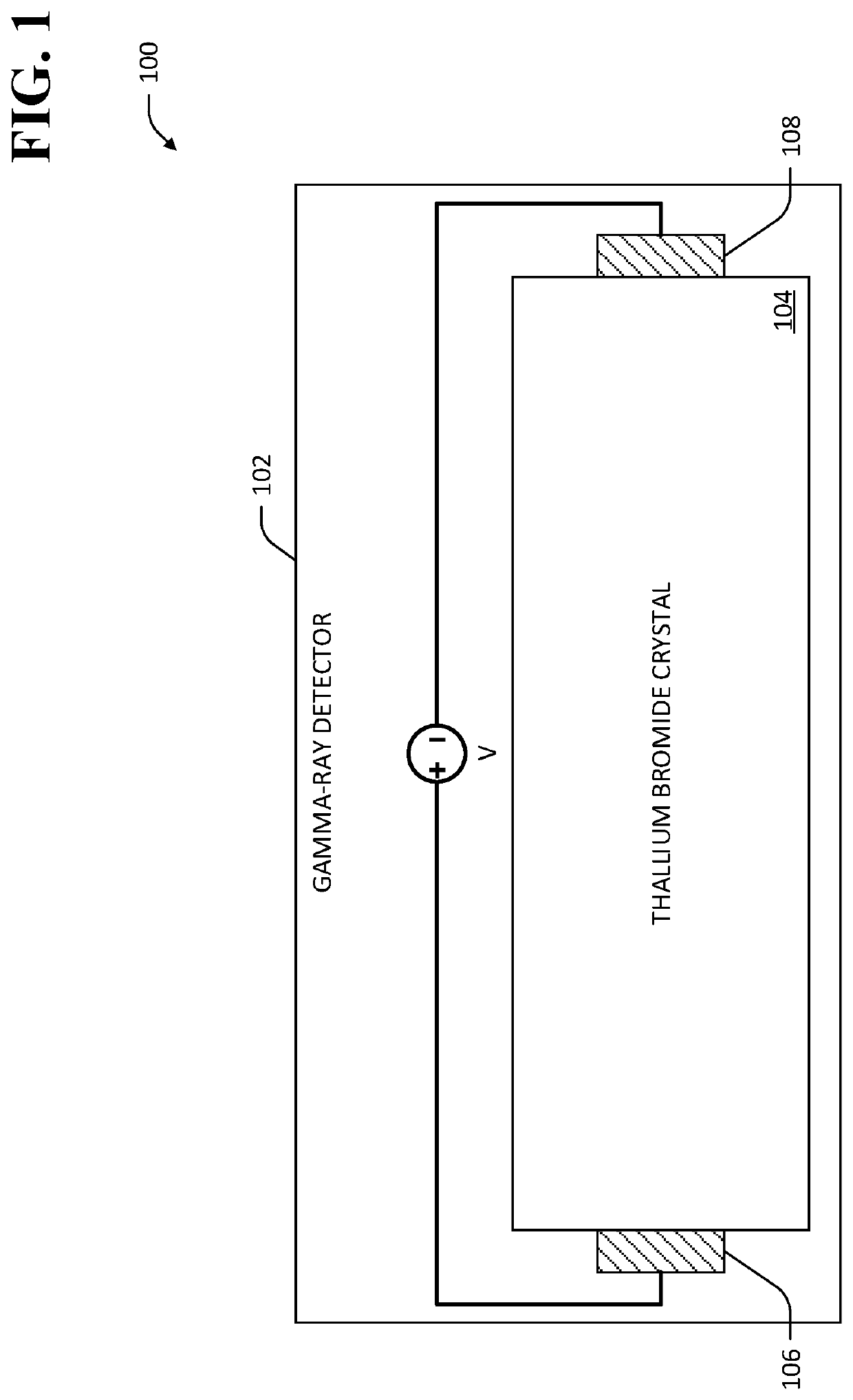
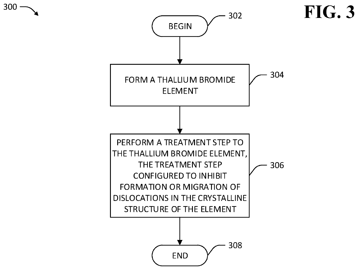
[0003]Thallium bromide (TlBr) is a wide bandgap, high-atomic number semiconductor, giving it certain desirable properties for use in gamma ray detection and spectroscopy. For example, as compared with commercially available cadmium zinc telluride (CZT), TlBr has higher atomic number that yields a higher photoelectric absorption, and wider bandgap that potentially yields lower dark current, enabling low-noise detectors with greater thickness than may be realized in CZT.
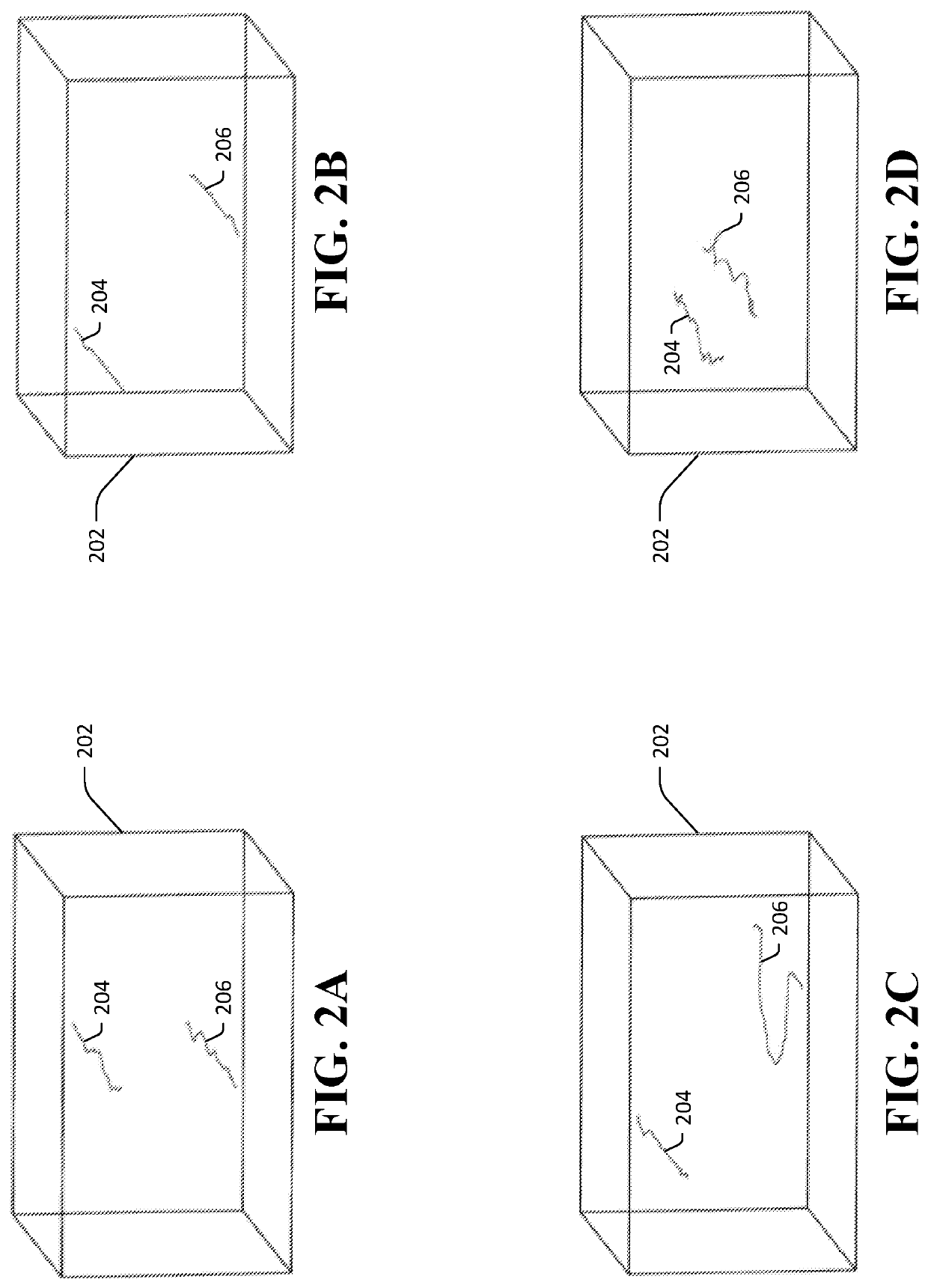
[0004]Conventional gamma ray detectors and other devices incorporating TlBr semiconductor elements have faced limited usefulness as a result of aging processes that generally cause TlBr-based detectors to become inoperable after less than 6 months of continuous use at room temper...
PUM
| Property | Measurement | Unit |
|---|---|---|
| crystalline structure | aaaaa | aaaaa |
| diffusion length | aaaaa | aaaaa |
| insoluble | aaaaa | aaaaa |
Abstract
Description
Claims
Application Information